|
|

Table Of Contents
4.1 Bidirectional Line Switched Rings
4.1.3 Adding and Dropping BLSR Nodes
4.2 Unidirectional Path Switched Rings
4.2.3 Adding and Dropping UPSR Nodes
4.4 Creating a Linear ADM Configuration
4.5 Path Protected Mesh Networks
4.6 Creating and Provisioning Circuits
4.6.1 Cross Connect Card Capacities
4.6.3 Creating Circuits With Multiple Drops
4.6.4 Creating Monitor Circuits
4.8 Loopbacks and Network Tests
4.9 Managing Multiple ONS 15454 Rings
4.10 Creating Diagnostic Files
4
Configuring Networks
This chapter provides procedures for configuring ONS 15454 rings and circuits including Bidirectional Line Switched Rings (BLSRs), Unidirectional Path Switched Rings (UPSRs), linear add-drop multiplexers (ADMs), circuits, Data Communication Channel (DCC) tunnels, and loopbacks.
4.1 Bidirectional Line Switched Rings
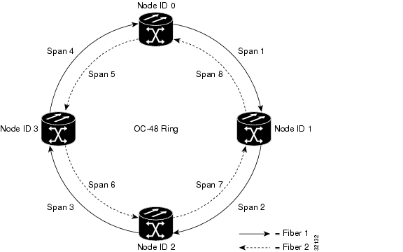
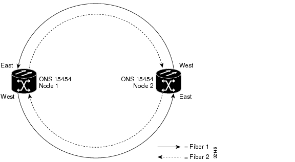
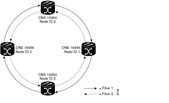
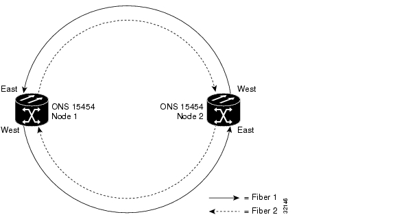
The ONS 15454 supports two-fiber BLSRs with up to 16 ONS 15454 nodes. BLSRs allocate half the available fiber bandwidth for protection. In an OC-48 BLSR, for example, STSs 1-24 are allocated to working traffic, and STSs 25-48 are allocated for protection. If a break occurs on one fiber, working traffic switches to the protection bandwidth (STSs 25-48) on the other fiber. Working traffic travels in one direction on STSs 1-24 on one fiber, and on STSs 1-24 in the opposite direction on the second fiber. Because the working and protection bandwidths must be equal, you can create only OC-12 and OC-48 BLSRs. Figure 4-1 shows a two-fiber OC-48 BLSR.
Figure 4-1 Four-Node, Two-Fiber OC-48 BLSR
SONET sends BLSR protection information over the K1 and K2 overhead bytes. The K bytes communicate failure conditions and actions taken between different nodes in the ring. Receiving nodes monitor the K bytes to determine when to switch the SONET signal to an alternate physical path. BLSRs are limited to a maximum of 16 nodes due to K byte node addressing requirements.
BLSR rings work well for distributed "mesh" and node-to-node traffic applications, such as interoffice networks and access networks. A BLSR node can terminate traffic fed from either side of the ring. Protection is provided by BLSR "standby bandwidth." Table 4-1 shows the bidirectional bandwidth capacities of two-fiber BLSRs.
Table 4-1 Two-Fiber BLSR Capacity
OC-12
STS1-6
STS 7-12
OC-48
STS 1-24
STS 25-48
24 x N - PT
1 N equals the number of ONS 15454 nodes configured as BLSR nodes.
2 PT equals the number of STS-1 circuits passed through an ONS 15454 node (capacity can vary depending on the traffic pattern).
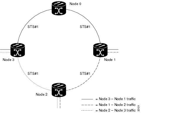
In BLSRs, bandwidth can be reused around the ring. The ONS 15454 can carry more traffic in networks with a distributed traffic pattern than a network with traffic flowing through one central hub. With a distributed traffic pattern, a BLSR can carry more traffic than a UPSR operating at the same optical rate.
Figure 4-2 shows an example of BLSR bandwidth reuse. The same STS carries three different traffic sets simultaneously on different spans on the ring: one set from Node 3 to Node 1, one from Node 1 to Node 2, and another from Node 2 to Node 3.
Figure 4-2 BLSR Bandwidth Reuse
4.1.1 Sample BLSR Application
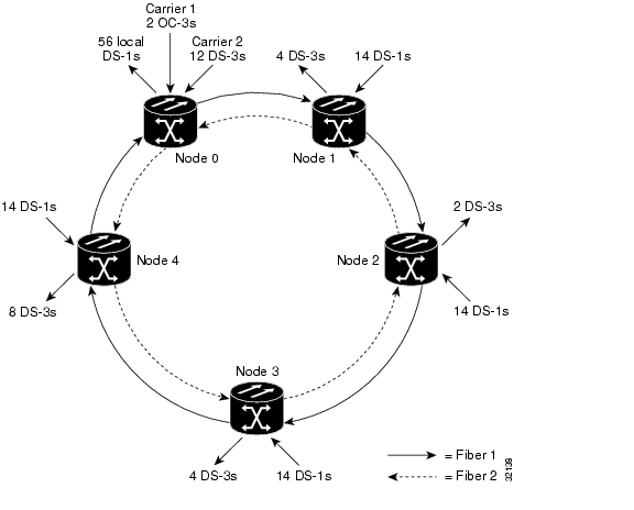
Figure 4-3 shows a sample BLSR implementation. A regional long-distance network connects to other carriers at Node 0. Traffic is delivered to the service provider's major hubs.
•
Carrier 1 delivers six DS-3s over two OC-3 spans to Node 0. Carrier 2 provides twelve DS-3s directly. Node 0 receives the signals and delivers them around the ring to the appropriate node.
•
•
Figure 4-3 Sample BLSR Application
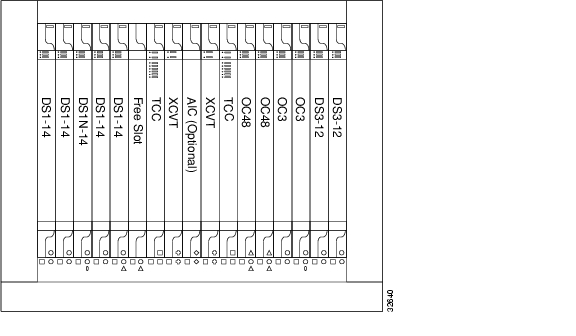
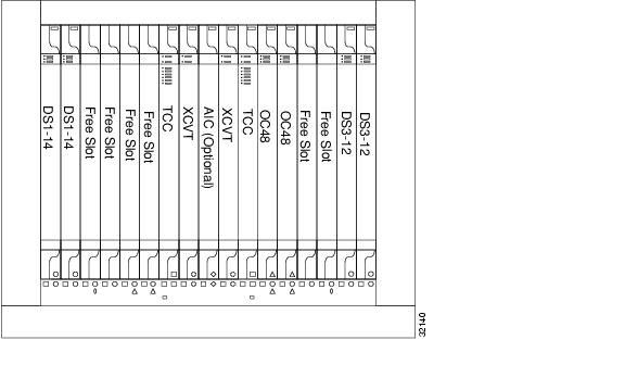
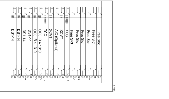
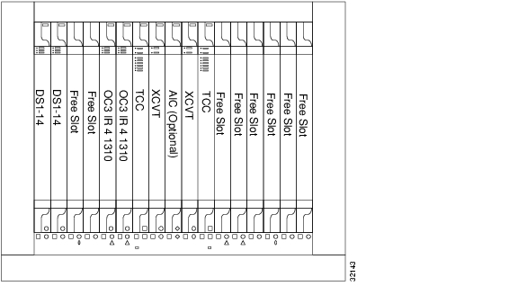
Figure 4-4 shows the shelf layout for Node 0, which has one free slot. Figure 4-5 shows the shelf layout for the remaining sites in the ring. In this BLSR configuration, an additional eight DS-3s at Node IDs 1 and 3 can be activated. An additional four DS-3s can be added at Node ID 4, and ten DS-3s can be added at Node ID 2. Each site has free slots for future traffic needs.
Figure 4-4 Sample Shelf Layout for Node 0 in Figure 4-3
Figure 4-5 Sample Shelf Layout for Nodes 1-4 in Figure 4-3
4.1.2 Setting Up BLSRs
To set up a BLSR, you perform five basic procedures:
•
•
•
•
•
The BLSR setup procedures in this section are for a two-fiber, two-node BLSR. However, you can apply the same setup principles to larger rings.
Procedure: Install the Optical Carrier Cards
Step 1
You can install the OC-12 cards in any slot, but the OC-48 cards can only be installed in Slots 5, 6, 12, or 13. Figure 4-6 shows a sample OC-48 BLSR. shows a sample card installation for a two-node, OC-48 BLSR.
Figure 4-6 Two Node OC-48 BLSR
Figure 4-7 Sample Shelf Setup for Two Node BLSR
Step 2
Step 3
Procedure: Create the BLSR DCC Terminations
Step 1
Step 2
Step 3
Step 4
Note
Step 5
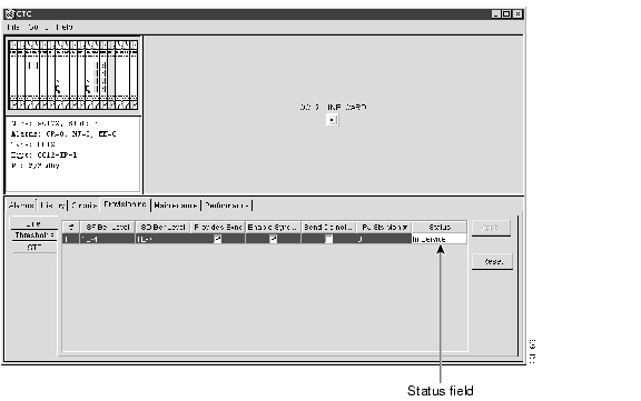
The slots/ports display under SDCC Terminations.
Step 6
Procedure: Enable the Optical Card Ports
Step 1
Step 2
Step 3
Step 4
Figure 4-8 Line Subtab
Step 5
Step 6
After configuring the SONET DCC, you set the timing for the node. For procedures, see the "Setup ONS 15454 Timing" section on page 3-31. For general information about ONS 15454 timing, including Synchronization Status Messaging, see the "Setting Up ONS 15454 Timing" section on page 3-29. After you configure the BLSR timing you can enable the BLSR ports, which is described in the following procedure.
Procedure: Configure the BLSR
Step 1
Step 2
Step 3
The Node ID identifies the node to the BLSR. Nodes in your BLSR must have different Node IDs. After you select a Node ID, the other BLSR fields are displayed.
Step 4
•
•
•
•
The east and west ports must be ports where you created SDCC terminations in the "Create the BLSR DCC Terminations" section. The fiber of the east port must plug into the fiber of the west port on an adjacent node, and the fiber of the east port must plug into the port of a west port. To avoid errors, use a system to assign BLSR ports. A common practice is to make the east port the furthest slot to the right and the west port the farthest left. For example, if you use Slots 4 and 14, Slot 14 is the east port and Slot 4 is the west port. Figure 4-9 shows the Ring subtab with the east and west ports selected.
Figure 4-9 Ring Subtab
Step 5
Step 6
Step 7
The node is added to the BLSR ring map. However, Default K alarms will display until all nodes in the ring are configured.
Step 8
Step 9
Step 10
(a)
(b)
(c)
(d)
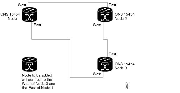
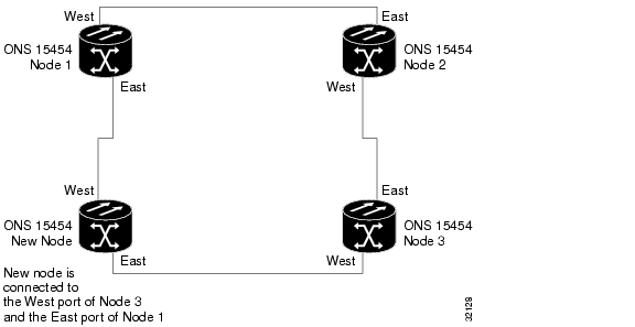
4.1.3 Adding and Dropping BLSR Nodes
This section provides procedures for adding and dropping BLSR nodes. To add or drop a node, you force a protection switch to route traffic away from the span where service will be performed.
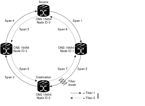
Figure 4-10 shows a three-node BLSR before the new node is added.
Note
Figure 4-10 Three Node BLSR Example
Procedure: Add a BLSR Node
Perform these steps on-site and not from a remote location.
Step 1
Step 2
Step 3
(a)
(b)
(c)
Performing a manual switch generates a manual equipment request alarm. This is normal.
Caution
Step 4
Step 5
(a)
(b)
(c)
Step 6
•
•
•
•
Step 7
(a)
(b)
Step 8
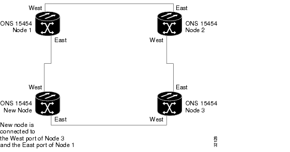
Figure 4-11 BLSR Example with Added Fourth Node
Step 9
Step 10
Step 11
Step 12
Step 13
Step 14
Step 15
(a)
(b)
Procedure: Drop a BLSR Node
Caution
Step 1
(a)
(b)
(c)
(d)
Note
Step 2
(a)
(b)
(c)
(d)
Caution
Step 3
Step 4
Step 5
Step 6
Step 7
Step 8
Step 9
(a)
(b)
(a)
(b)
Step 10
Step 11
Step 12
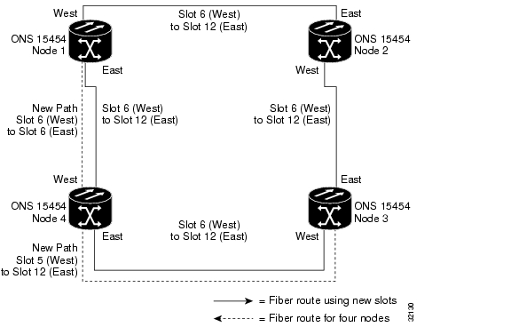
4.1.4 Moving BLSR Trunk Cards
Caution
Caution
shows a four node OC-48 BLSR made up of Node 1, Node 2, Node 3, and Node 4. Node 4 is temporarily removed from the active BLSR, while the OC-48 card in Slot 6 moves to Slot 5 and the OC-48 card in Slot 12 moves to Slot 6.
Figure 4-12 BLSR Trunk Card Switchover Example
Procedure: Move a BLSR Trunk Card
Use the following steps to move one BLSR trunk card to a different slot. Use this procedure for each card you want to move. Although the procedure is for OC-48 BLSR trunk cards, you can use the same procedure for OC-12 cards.
Note
Step 1
(a)
(b)
(c)
When you perform a manual switch, a manual equipment request alarm is generated. This is normal.
Caution
(d)
(e)
(f)
Step 2
Step 3
Step 4
Figure 4-13 Circuits Tab
Step 5
(a)
(b)
(c)
Step 6
(a)
(b)
Step 7
(a)
(b)
(c)
Step 8
Step 9
(a)
(b)
Step 10
Step 11
Step 12
Step 13
(a)
(b)
(c)
(d)
Step 14
Step 15
For more information about circuit provisioning, see the "Creating and Provisioning Circuits" section.
Step 16
4.2 Unidirectional Path Switched Rings
UPSRs provide duplicate fiber paths around the ring. Working traffic flows in one direction and protection traffic flows in the opposite direction. If a problem occurs in the working traffic path, the receiving node switches to the path coming from the opposite direction.
Figure 4-14 shows a basic UPSR configuration. If Node ID 0 sends a signal to Node ID 2, the working signal travels on the working traffic path through Node ID 1. The same signal is also sent on the protect traffic path through Node ID 3. If a fiber break occurs ( Figure 4-15), Node ID 2 switches its active receiver to the protect signal coming through Node ID 3.
Figure 4-14 Basic UPSR Configuration
Figure 4-15 UPSR Fiber Break
Because each traffic path is transported around the entire ring, UPSRs are best suited for networks where traffic concentrates at one or two locations and is not widely distributed. UPSR ring capacity is equal to its bit rate. Services can originate and terminate on the same UPSR, or they can be passed to an adjacent access or interoffice ring for transport to the service-terminating location.
CTC automates ring configuration. UPSR traffic is defined within the ONS 15454 on a circuit-by-circuit basis. If a path-protected circuit is not defined within a 1+1 or BLSR line protection scheme and path protection is available and specified, CTC uses UPSR as the default.
4.2.1 Sample UPSR Application
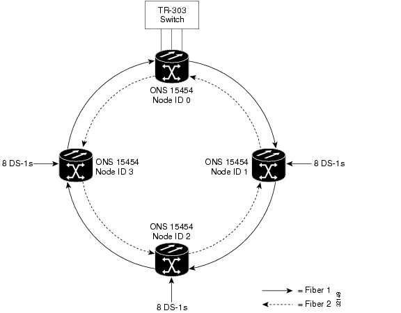
Figure 4-16 shows a common UPSR application. OC-3 optics provide remote switch connectivity to a host TR-303 switch. In the example, each remote switch requires eight DS-1s to return to the host switch. and show the shelf layout for each site.
Figure 4-16 Sample OC-3 UPSR Application
Node ID 0 has four DS1-14 cards to provide 56 active DS-1 ports. The other sites only require two DS1-14 cards to handle the eight DS-1s to and from the remote switch. You can use the other half of each ONS 15454 shelf to provide support for a second or third ring to other existing or planned remote sites.
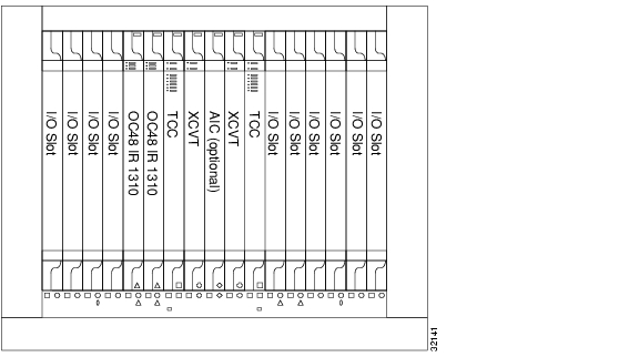
In this sample OC-3 UPSR, Node 0 contains four DS1-14 cards and two OC3 IR 4 1310 cards. Six free slots also exist in this setup and can be provisioned with cards or left empty. Figure 4-17 shows the shelf setup for these cards.
Figure 4-17 Node ID 0 Layout for Sample OC-3 UPSR
In this sample OC-3 UPSR, Nodes 1 to 3 each contain two DS1-14 cards and two OC3 4 IR 1310 cards. Eight free slots exist. They can be provisioned with other cards or left empty. Figure 4-18 shows the shelf setup for this configuration sample.
Figure 4-18 Node ID 1-3 Layout for Sample OC-3 UPSR
4.2.2 Setting Up a UPSR
To set up a UPSR, you perform four basic procedures:
•
•
•
•
After you enable the ports, you set up the UPSR circuits. UPSR signal thresholds are set at the circuit level. For procedures on creating UPSR circuits, see the "Creating and Provisioning Circuits" section.
Procedure: Install the Optical Carrier Cards
Step 1
Step 2
Figure 4-19 Sample Two Node OC-48 UPSR
Figure 4-20 Sample Two Node OC-48 UPSR Shelf Setup
Procedure: Configure the UPSR DCC Terminations
Step 1
Step 2
Step 3
Step 4
Note
Step 5
The slots/ports display under SDCC Terminations.
Step 6
After configuring the SONET DCC, set the timing for the node. For procedures, see the "Setup ONS 15454 Timing" section on page 3-31. For general information about ONS 15454 timing, see the "Setting Up ONS 15454 Timing" section on page 3-29. After configuring the timing, enable the UPSR ports as described in the following procedure.
Procedure: Enable the UPSR Ports
Step 1
Step 2
Step 3
Step 4
Step 5
You configured a UPSR for one node. Use the same procedure to configure the additional nodes. To create path protected mesh networks, see the "Path Protected Mesh Networks" section. To create circuits, see the "Creating and Provisioning Circuits" section.
4.2.3 Adding and Dropping UPSR Nodes
This section provides procedures for adding and dropping nodes in an ONS 15454 UPSR configuration. To add or drop a node, you manually switch traffic on the affected spans to route traffic away from the area of the ring where service will be performed. Use the selector maintenance option to switch traffic from a UPSR span at different protection levels. The selector maintenance option is useful when you need to temporarily reroute traffic from a UPSR span to add or drop nodes, perform maintenance, or perform other operations. Figure 4-21 shows a three-node UPSR before a fourth node is added.
Figure 4-21 Three Node UPSR
Procedure: Switch UPSR Traffic
Step 1
Step 2
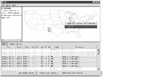
Figure 4-22 Span Shortcut Menu
Step 3
•
•
•
•
Caution
Figure 4-23 Circuits on Span Dialog
Step 4
Step 5
Step 6
Procedure: Add a UPSR Node
Note
Step 1
•
•
•
Step 2
Step 3
Caution
Step 4
(a)
(b)
Step 5
Figure 4-24 UPSR Example With Fourth Node
Note
Step 6
Step 7
Step 8
Step 9
Step 10
Step 11
Procedure: Drop a Node
Caution
Step 1
Caution
Step 2
(a)
(b)
(c)
(d)
Step 3
Step 4
Step 5
Step 6
Note
Step 7
(a)
(b)
(c)
4.3 Subtending Rings
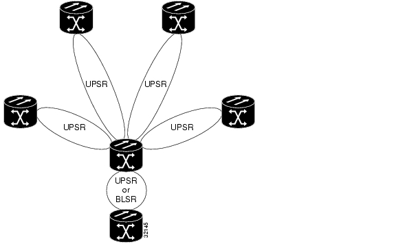
Because the ONS 15454 supports up to ten SONET DCCs, one ONS 15454 can terminate and groom five UPSR rings or four UPSR rings and one BLSR ring. (If you tunnel DCCs, this number drops by one ring for each DCC tunnel. See the "DCC Tunneling" section.) Subtending rings from a single ONS 15454 reduces the number of shelves and cards required, and reduces external shelf-to- shelf cabling. Figure 4-25 shows an ONS 15454 with multiple subtending rings.
Note
Figure 4-25 ONS 15454 With Multiple Subtending Rings
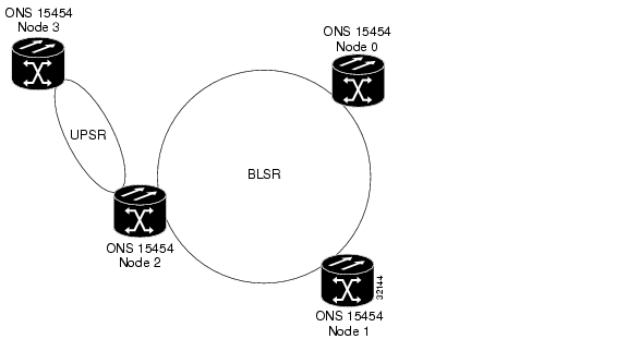
This section shows how to subtend a UPSR from a BLSR. To subtend multiple rings, repeat the following procedure for each ring. Figure 4-26 shows a UPSR subtending from a BLSR. In this example, Node 2 is the only node serving both the BLSR and UPSR. Some Node 2 slots are dedicated to BLSR and others to UPSR.
Figure 4-26 Multiple Subtending Rings
Procedure: Subtend a UPSR from a BLSR
Step 1
Step 2
Step 3
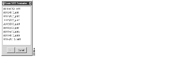
The Create SDCC Termination dialog is displayed ( Figure 4-27).
Figure 4-27 Create SDCC Termination dialog
Step 4
Step 5
Step 6
The selected slots/ports are displayed under SDCC Terminations.
Step 7
(a)
(b)
(c)
Step 8
Step 9
Step 10
Procedure: Subtend a BLSR from a UPSR
Step 1
Step 2
Step 3
The Create SDCC Termination dialog is displayed.
Step 4
Step 5
Step 6
The selected slots/ports are displayed under SDCC Terminations.
Step 7
(a)
(b)
The Node ID identifies the node to the BLSR. Nodes in your BLSR must have different Node IDs. After you select a Node ID, the other BLSR fields are displayed.
(c)
–
–
–
–
(d)
Step 8
(a)
(b)
(c)
(d)
(e)
Step 9
Step 10
Step 11
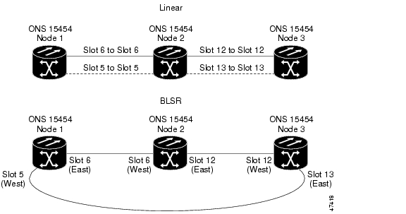
4.4 Creating a Linear ADM Configuration
You can configure ONS 15454s as a line of add-drop multiplexers (ADMs) by configuring one set of optical cards as the working path and a second set as the protect path. Unlike rings, linear ADMs require that the optical cards at each node be in 1+1 protection to ensure that a break to the working line is automatically routed to the protect line.
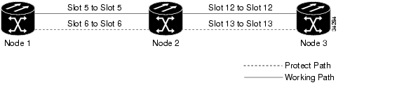
shows three ONS 15454s in a linear ADM configuration. Working traffic flows from Slot 6 of Node 1 to Slot 6 of Node 2, and from Slot 12 of Node 2 to Slot 12 of Node 3. You create the protect path by placing Slot 6 in a 1+1 protection with Slot 5 at Nodes 1 and 2, and Slot 12 in 1+1 protection with Slot 13 at Nodes 2 and 3.
Figure 4-28 Linear ADM
Procedure: Create a Linear ADM
Complete the following steps for each node that will be included in the linear ADM.
Step 1
Step 2
Step 3
Step 4
(a)
(b)
(c)
Note
Step 5
Step 6
(a)
(b)
(c)
Repeat Step 6 for each optical card connected to the linear ADM.
Procedure: Convert a Linear ADM to UPSR
The following procedures describe how to convert a three-node linear ONS 15454 ADM to a UPSR.
Caution
Step 1
Step 2
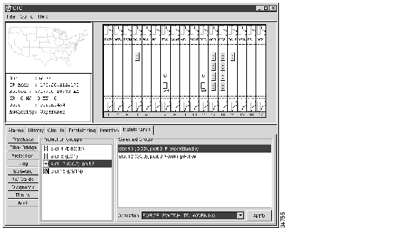
Figure 4-29 Maintenance>Protection Subtab
Step 3
(a)
(b)
(c)
(d)
(e)
Repeat Step 3 for each group listed in Protection Groups.
Step 4
(a)
(b)
(c)
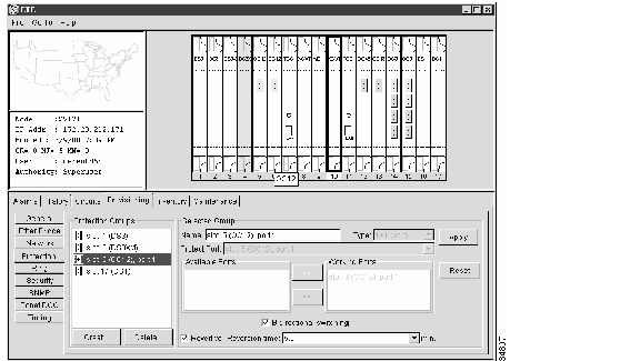
Figure 4-30 Provisioning>Protection Subtab
Step 5
Figure 4-31 Linear to UPSR Conversion
Step 6
Step 7
(a)
(b)
(c)
(d)
(e)
(f)
(g)
Step 8
Step 9
Step 10
Step 11
Step 12
Step 13
Step 14
Note
Step 15
Figure 4-32 Network View with Ring
Procedure: Convert a Linear ADM to a BLSR
The following procedures describe how to convert a three-node linear ONS 15454 ADM to a BLSR.
Caution
Step 1
Step 2
Step 3
(a)
(b)
(c)
(d)
(e)
Repeat Step 3 for each group listed in Protection Groups.
Step 4
(a)
(b)
(c)
Step 5
Figure 4-33 Linear to BLSR Conversion
Step 6
Figure 4-33 example, the fiber between Node 1/Slot 5 and Node 2/Slot 5 is rerouted to connect Node 1/Slot 5 to Node 3/Slot 13.Step 7
(a)
(b)
(c)
(d)
(e)
(f)
(g)
Step 8
Step 9
Step 10
Step 11
Step 12
Step 13
Step 14
(a)
(b)
(c)
Note
Step 15
(a)
(b)
The Node ID identifies the node to the BLSR. Nodes in your BLSR must have different Node IDs. After you select a Node ID, the other BLSR fields are displayed.
(c)
–
–
–
–
(d)
(e)
(f)
Step 16
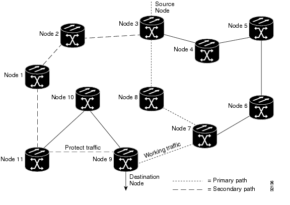
4.5 Path Protected Mesh Networks
ONS 15454 networks give you the option to set up path protected mesh networks (PPMN). PPMN extends the protection scheme of UPSR from the basic ring configuration to the meshed architecture of several interconnecting rings. Typical UPSR protection creates two separate routes between source and destination nodes on a single UPSR. PPMN does this for source and destination nodes that do not lie on the same ring but link together through a network of meshed connections. When applied to a single ring, PPMN uses the same paths as the Telcordia-specified UPSR.
PPMN connects the source and destination of a circuit over two diverse paths through a network of single or multiple meshed rings. These two routes form a circuit-level UPSR. The source sends traffic on each of the diverse routes to the destination node, where the destination node uses the active route or switches to the standby route.
Note
When you check the "Fully protect path" box during the normal A to Z provisioning process, PPMN provisions automatically in CTC. Choosing this option establishes an alternate route for the circuit in addition to the normally provisioned route. The second route or the protected path follows a unique second path through the network between the source and destination and sets up a second set of cross-connections. You can do this routing manually as well.
Figure 4-34 shows an example of PPMN. In the example, A to Z provisioned Node 3 as the source node and Node 9 as the destination node. The ONS 15454 CTC determined that the shortest route between the two end nodes passes through Node 8 and Node 7, shown by the dotted line. A to Z provisioning then automatically created cross-connections at each of the four nodes, 3, 8, 7, and 9, to provide the route for working traffic.
When the protected circuit box is checked, PPMN establishes a second unique route between Nodes 3 and 9 and automatically creates cross-connections at each of the five nodes, 3, 2, 1, 11, and 9 as illustrated by the dashed line. If a signal failure occurs on the primary path, traffic switches to the second, or protected circuit path. In this example, Node 9 switches from the traffic coming in from Node 7, to the traffic coming in from Node 11 and service resumes. The switch occurs within
50 milliseconds.Figure 4-34 Path Protected Mesh Network Example
PPMN also allows spans of different SONET line rates to be mixed together in "virtual rings." Figure 4-35 shows Nodes 1, 2, 3, and 4 forming a standard OC-48 ring. Nodes 5, 6, 7, and 8 link to the backbone ring through OC-12 fiber. The "virtual ring" formed by Nodes 5 - 6 - 7 - 8 uses both OC-48 and OC-12.
Figure 4-35 PPMN Virtual Ring
4.6 Creating and Provisioning Circuits
You can create STS, VT1.5, and Ethernet circuits across and within ONS 15454 nodes and assign. circuits different attributes. For example, you can:
•
•
•
Note
•
•
•
•
4.6.1 Cross Connect Card Capacities
The ONS 15454 XC and XCVT cards perform the port-to-port time division multiplexing. XC cards perform STS switching; XCVT cards perform STS and VT1.5 switching. All TDM traffic consumes XC and XCVT bandwidth, even traffic that originates and terminates on the same ONS 15454. For example, each OC-12 card and the 12-port DS3-12 card consume 12 STS ports.
shows the terminating STS and STS port-connection capacities of the XC and XCVT cards. shows the terminating STS and VT1.5 connection capacities.
Table 4-2 XC and XCVT Card Capacity: STSs (Bidirectional)
XC
288
144
XCVT
288
144
Table 4-3 XC and XCVT Card Capacity: VT1.5s (Bidirectional)
XC
0
0
XCVT
24 (672 VT1.5s)
336
When VT1.5 circuits are routed through ONS 15454 nodes, the number of VTs used within the XCVT cross-connect matrix depends on the protection scheme of the node. VT use is slightly higher at the source and drop nodes in 1+1 protection and in UPSRs than in BLSRs. shows an example of VT use within an XCVT at the source and drop nodes.
Table 4-4 VT Use Example
1 + 1
31
1) I/O card
2) Trunk card (working)
3) Trunk card (protect)
UPSR
3*
1) I/O card
2) Trunk card (working)
3) Trunk card (protect)
BLSR
2
1) I/O card
2) Trunk card (working)
1 Source and drop nodes; two VT ports are used at pass-through nodes
4.6.2 VT Tunnels
You can tunnel VT1.5 circuits through ONS 15454 nodes. VT1.5 tunnels provide two benefits:
•
•
When planning VT1.5 circuits, weigh the benefits of using tunnels with the need to maximize STS capacity. For example, a VT1.5 tunnel between Node 1 and Node 4 passing (transparently) through Node 2 and Node 3 is advantageous if:
•
•
•
However, if the Node 1 - Node 4 tunnel carries only a few VT1.5 circuits, creating a regular VT1.5 circuit between Nodes 1, 2, 3, and 4 might maximize STS capacity.
When you create a VT1.5 circuit, CTC checks to see whether a tunnel already exists between source and drop nodes. If a tunnel exists, CTC checks the tunnel capacity. If capacity is sufficient, CTC routes the circuit on the existing tunnel. If a tunnel does not exist, or if an existing tunnel does not have sufficient capacity, CTC displays a dialog asking whether you want to create a tunnel. Before you create the tunnel, review the existing tunnel availability, keeping in mind future bandwidth needs. In some cases, manually routing a circuit might make more sense than creating a new tunnel.
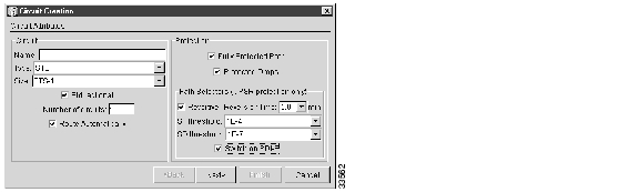
Procedure: Create a Circuit
Step 1
Step 2
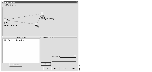
Figure 4-36 Circuit Creation Dialog
Step 3
•
•
•
•
•
•
•
•
Step 4
•
•
•
•
•
Step 5
Step 6
Options include node, slot, port, STS, and VT/DS-1. The options displayed depend on the circuit type and circuit properties you selected and the cards installed in the node. For example, if the node does not have an XCVT card, VT circuits are not available for selection. For Ethergroups, see the "ONS 15454 Ethernet Circuit Configurations" section on page 7-16.
Click Use Secondary Source if you need to create a UPSR bridge/selector circuit entry point in a multivendor UPSR ring.
Step 7
Step 8
Step 9
Figure 4-37 Circuit Path Selection Dialog
(a)
(b)
(c)
The span turns blue.
(d)
When provisioning a BLSR circuit, you only need to select one BLSR path from the source to the drop. If you are provisioning a UPSR, you can only select unprotected spans as paths. BLSR and 1+1 protected spans are not allowed. When selecting UPSR spans, select two different paths from source to drop. In Figure 4-37, the arrows would point from Node_1 to Node_2, Node_2 to Node_3, and from Node_1 to Node_3 (protect span).
Caution
(e)
Step 10
Step 11
If you entered more than 1 in Number of Circuits in the Circuit Attributes dialog, the Circuit Source dialog is displayed so you can create the remaining circuits. Otherwise, you are finished provisioning a circuit.
Note
4.6.3 Creating Circuits With Multiple Drops
Unidirectional circuits can have multiple drops for use in broadcast circuit schemes. In broadcast scenarios, one source transmits traffic to multiple destinations, but traffic is not returned back to the source.
Note
Procedure: Create a Circuit with Multiple Drops
Step 1
Step 2
Step 3
Step 4
Step 5
Step 6
Step 7
4.6.4 Creating Monitor Circuits
You can set up secondary circuits to monitor traffic on primary circuits. You can create monitor circuits for bidirectional circuits only. For unidirectional circuits, simply create a drop to the port where the test equipment is attached. shows an example. At Node 1, a VT1.5 is dropped from Port 1 of an EC1-12 card. To monitor the VT1.5 traffic, test equipment is plugged into Port 2 of the EC1-12 and CTC is used to provision a circuit monitor to Port 2. Circuit monitors are one-way. The monitor in shows VT1.5 traffic received by the EC1-12. To monitor traffic sent from Node 1, a circuit monitor needs to be set up at Node 2.
Note
Figure 4-38 Monitor Circuit Example
Procedure: Set Up a Monitor Circuit
Step 1
Step 2
Step 3
Step 4
The Monitors tab displays ports that you can use to monitor the circuit selected in Step 3.
Figure 4-39 Monitors Tab
Step 5
Step 6
Step 7
Step 8
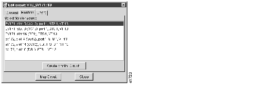
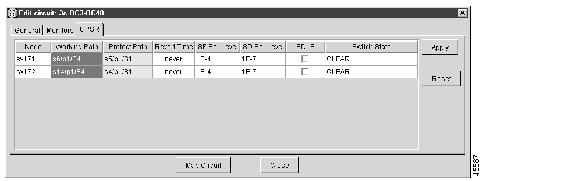
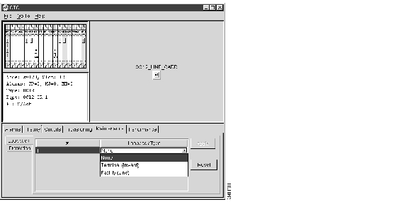
4.6.5 Editing UPSR Circuits
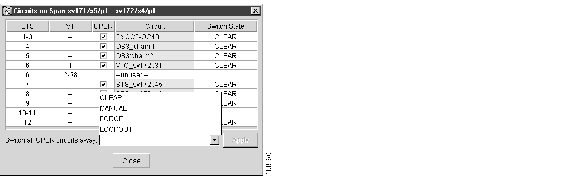
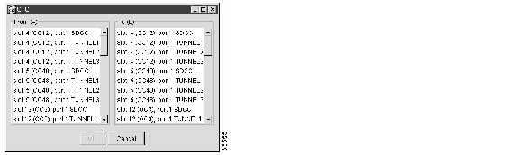
To change UPSR selectors and switch protection paths, use the Edit Circuits dialog ( ). You can view the UPSR circuit's working and protection paths, edit the reversion time, edit the Signal Fail/Signal Degrade thresholds, turn PDI-P on or off, and perform maintenance switches on the circuit selector. You can also display a map of the UPSR circuits to better see circuit flow between nodes.
Figure 4-40 Edit Circuit Dialog - UPSR Tab
Procedure: Edit UPSR Circuits
Step 1
Step 2
Step 3
Step 4
Step 5
•
•
•
•
•
CLEAR—removes a previously-set switch command.
LOCKOUT OF PROTECT—prevents traffic from switching to the protect circuit path.
FORCE TO WORKING—forces traffic to switch to the working circuit path, regardless of whether the path is error free.
FORCE TO PROTECT—forces traffic to switch to the protect circuit path, regardless of whether the path is error free.
MANUAL TO WORKING—switches traffic to the working circuit path when the working path is error free.
MANUAL TO PROTECT—switches traffic to the protect circuit path when the protect path is error free.
Caution
Step 6
Step 7
4.7 DCC Tunneling
SONET provides four data communications channels (DCCs) for network element operations, administration, maintenance, and provisioning: one on the SONET Section layer and three on the SONET Line layer. The ONS 15454 uses the Section DCC (SDCC) for ONS 15454 management and provisioning.
You can use the Line DCCs (LDCCs) and the SDCC (when the SDCC is not used for ONS 15454 DCC terminations) to tunnel third-party SONET equipment SDCCs across ONS 15454 networks. To create a DCC tunnel, you connect the tunnel end points from one ONS 15454 optical port to another. DCC traffic is forwarded transparently, byte-for-byte, across the ONS 15454 network. Each ONS 15454 can support up to 32 DCC tunnel connections. shows the DCC tunnels that you can create.
Table 4-5 DCC Tunnels
SDCC
Section
D1 - D3
Yes
Yes
Yes
Tunnel 1
Line
D4 - D6
No
Yes
Yes
Tunnel 2
Line
D7 - D10
No
Yes
Yes
Tunnel 3
Line
D11 - D12
No
Yes
Yes
1 You cannot use Ports 2 and 4 on OC-3 cards for DCC tunnels.
4.7.1 Creating DCC Tunnels
A DCC tunnel is a series of connection points that map a third-party equipment SDCC to ONS 15454 LDCCs. DCC tunnel end points are defined by slot, port, and DCC type (SDCC, Tunnel 1, Tunnel 2, or Tunnel 3). You can link an SDCC to an LDCC (Tunnel 1, Tunnel 2, or Tunnel 3), and an LDCC to an SDCC. You can also link LDCCs to LDCCs and link SDCCs to SDCCs.
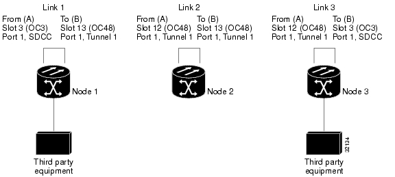
Figure 4-41 shows a DCC tunnel example. Third-party equipment is connected to OC-3 cards at Node 1, Slot 3, Port 1, and Node 3, Slot 3, Port 1. Each ONS 15454 node is connected by OC-48 trunk cards. In the example, three tunnel connections are created, one at Node 1 (OC-3 to OC-48), one at Node 2 (OC-48 to OC-48), and one at Node 3 (OC-48 to OC-3).
Figure 4-41 DCC Tunnel Example
Procedure: Provision a DCC Tunnel
Step 1
Step 2
Step 3
Step 4
Note
Figure 4-42 Create DCC Tunnel Connection Dialog
Step 5
Step 6
(a)
(b)
(c)
(d)
DCC Provisioning is now complete for one slot/port. Repeat these steps for all slots/ports that are part of the DCC tunnel, including any intermediate nodes that will pass traffic through third party equipment. The procedure is confirmed when the third party network elements successfully communicate over the newly established DCC tunnel.
4.8 Loopbacks and Network Tests
Use loopbacks and hairpins to test newly-created circuits before adding live traffic or to logically isolate the source of a network failure. All ONS 15454 I/O cards, except Ethernet cards, allow loopbacks and hairpins.
4.8.1 Network Test Types
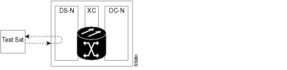
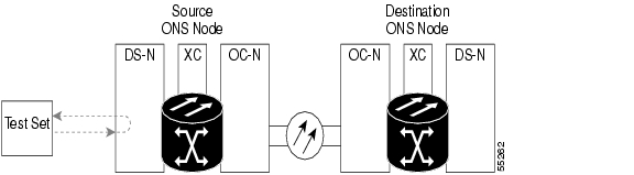
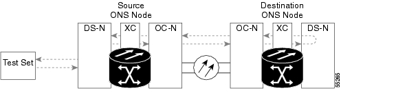
Facility loopbacks test the line interface unit (LIU) of a card, the backplane, and cabling. You put a facility loopback on a card and use a test set to run traffic over the loopback. A successful facility loopback eliminates the LIU of the card, backplane, and cabling plant as the cause or potential cause of a network problem. shows a facility loopback on a DS-N card.
Figure 4-43 The facility loopback process
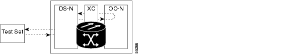
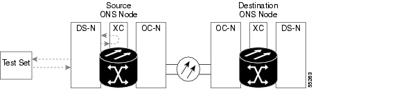
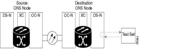
Terminal loopbacks test a circuit path through the XC card and loop back from the card that the terminal loopback is testing. shows a terminal loopback set on an OC-N card. The test set traffic comes in on the DS-N card and goes through the XC card to the OC-N card. The terminal loopback on the OC-N card turns the signal around before it reaches the LIU and sends it through the XC card to the DS-N card. This test verifies that the XC card and circuit paths are valid, but does not test the LIU on the OC-N card. To test the LIU on an OC-N card, connect an optical test set to the OC-N card ports and perform a facility loopback or use a loopback or hairpin on a card that is farther along the circuit path.
Figure 4-44 The terminal loopback process
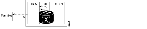
Hairpin circuits bring traffic in and out on a DS-N port instead of sending the traffic onto the OC-N. A hairpin loops back only the specific STS or VT circuit and does not cause an entire OC-N port to loopback, which would drop all traffic on the OC-N port. The hairpin allows you to test a circuit on nodes running live traffic.
Figure 4-45 The hairpin circuit process
4.8.2 Network Test Procedures
Facility loopbacks, terminal loopbacks, and hairpin circuits are often used together to test the circuit path through the network or to logically isolate a fault. Performing a network test at each point along the circuit path systematically eliminates possible points of failure. In our example, we test a DS-N circuit on a two node BLSR. Using a series of facility loopbacks, terminal loopbacks, and hairpins, we trace the path of the circuit and eliminate possible points of failure.
A logical progression of five network test procedures apply to this scenario: a facility loopback on the source node DS-N card, a hairpin on the source node DS-N card, a hairpin on the destination node OC-N card, a terminal loopback to the destination node DS-N card, and a facility loopback to the destination DS-N card.
Procedure: Perform a Facility Loopback on a Source DS-N Card
The first loopback test is a facility test performed on the first card in the circuit; in this example, the DS1-14 card in source node. Completing a successful facility loopback on this card eliminates the cabling, DS-N card, and the backplane as possible failure points.
Figure 4-46 Facility loopback on a source DS-N card
Caution
Note
Step 1
To perform a hard loop, bridge the test set transmit (Tx) and receive (Rx) terminals with a cable and send traffic across this loop to ensure that the test set works.
Step 2
Step 3
Step 4
Step 5
Figure 4-47 Performing a facility loopback
Step 6
Step 7
Note
Step 8
Step 9
Step 10
(a)
–
–
(b)
Step 11
Step 12
(a)
(b)
(c)
(d)
Step 13
(a)
(b)
(c)
(d)
Step 14
(a)
(b)
(c)
(d)
(e)
(f)
(g)
Step 15
Procedure: Perform a Hairpin on a Source Node
The second loopback test is a hairpin circuit performed on the first XC card in the circuit. Completing a successful loopback through this card eliminates the possibility that the source XC card is the reason for the faulty circuit.
Figure 4-48 Hairpin on a source node
Note
Step 1
To perform a hard loop, bridge the test set transmit (Tx) and receive (Rx) terminals with a cable and send traffic across this loop to make the test set work.
Step 2
Step 3
Step 4
Step 5
Step 6
Step 7
Step 8
Step 9
Step 10
Step 11
Step 12
Step 13
Step 14
Step 15
Step 16
Caution
Step 17
(a)
(b)
(c)
Step 18
(a)
Note
(b)
(c)
(d)
Note
(e)
Now the test set traffic goes through the alternate XC card.
(f)
(g)
(h)
–
–
–
–
(i)
(j)
(k)
(l)
Procedure: Perform a Hairpin on a Destination Node
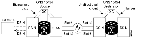
The third test is a hairpin circuit on the XC card in the destination node. To perform this test, first create a bidirectional circuit from the source DS-N card to the source OC-N node in the transmit direction. Creating the bidirectional circuit and completing a successful hairpin eliminates the possibility that the source and destination OC-N cards, the destination XC card, or the fiber span is responsible for the faulty circuit.
Figure 4-49 Hairpin on a destination node
Step 1
Note
Step 2
Step 3
Step 4
Step 5
Step 6
Step 7
Step 8
Step 9
Step 10
Step 11
Step 12
Step 13
Step 14
Step 15
Step 16
Step 17
Step 18
Step 19
Step 20
Step 21
Step 22
Step 23
Step 24
Step 25
Step 26
Step 27
Step 28
Caution
Step 29
(a)
(b)
(c)
Step 30
(a)
(b)
(c)
Note
(d)
Now the test set traffic routes through the alternate XC card.
(e)
(f)
(g)
–
–
–
–
(h)
(i)
(j)
The test set traffic routes through the alternate XC card rather than the original XC card.
(k)
(l)
(m)
–
–
–
–
(n)
(o)
Step 31
(a)
(b)
(c)
(d)
(e)
If the test traffic is not received or is poor quality and the OC-N card is a known good card, then the fiber span is suspect.
Step 32
Step 33
Step 34
Step 35
Step 36
Step 37
Step 38
Step 39
Procedure: Perform a Terminal Loopback on a Destination DS-N Card
The fourth test is a terminal loopback performed on the fourth I/O card in the circuit; in this example the DS-N card in the destination node. First create a bidirectional circuit that starts on the source node DS-N port and terminates on the destination node DS-N port, then proceed with the terminal loopback test. Completing a successful terminal loopback to a destination node DS-N card eliminates the possibility that this card is responsible for the faulty circuit.
Figure 4-50 Terminal loopback on a destination DS-N card
Caution
Step 1
To perform a hard loop, bridge the test set transmit (Tx) and receive (Rx) terminals with an appropriate cable and send traffic across the loop to ensure the test set works.
Step 2
Step 3
Step 4
Step 5
Step 6
Step 7
Step 8
Step 9
Step 10
Step 11
Step 12
Step 13
Step 14
Step 15
Step 16
Step 17
Note
Note
Step 18
Step 19
Step 20
Step 21
(a)
(b)
(c)
Procedure: Perform a Facility Loopback on a Destination DS-N Card
The final test is a facility loopback performed on the last card in the circuit; in this case the DS-N card in the destination node. Completing a successful facility loopback on this card eliminates the possibility that the destination node cabling, DS-N card, LIU, or backplane is responsible for a faulty circuit.
Figure 4-51 Facility loopback on a destination DS-N card
Caution
Note
Step 1
To perform a hard loop on the test set, bridge the test set transmit (Tx) and receive (Rx) terminals with an appropriate cable and send traffic across this loop to make the test set works.
Step 2
Step 3
Step 4
Note
Step 5
Step 6
Step 7
Note
Step 8
Step 9
Step 10
(a)
–
–
(b)
Step 11
Step 12
(a)
(b)
(c)
(d)
(e)
Step 13
(a)
(b)
(c)
(d)
Step 14
(a)
(b)
(c)
(d)
(e)
(f)
(g)
Step 15
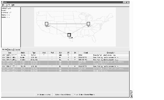
4.9 Managing Multiple ONS 15454 Rings
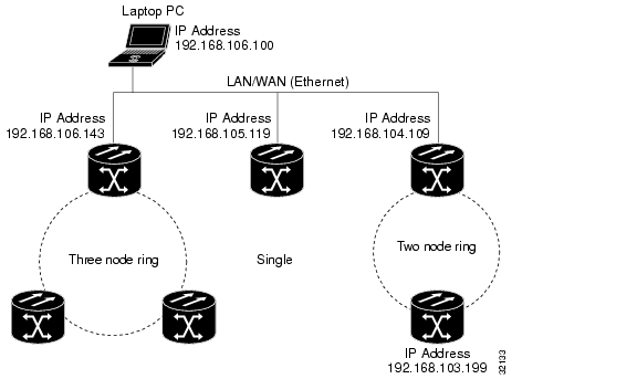
A small modification to the CMS.INI file enables CTC to manage multiple rings or nodes that are connected only by Ethernet and not interconnected by fiber or the DCC. Figure 4-52 shows a multiple ONS 15454 ring. An ONS 15454 with an unmodified CMS.INI file can only manage the ONS 15454 that the PC dialed directly into and the three node ring attached to that ONS 15454. The file cannot manage the single node and two-node ring that are not optically connected to the dialed into ONS 15454. However, you can modify the CMS.INI file to manage the additional single node and two node ring.
Figure 4-52 CTC Multiple Ring Management
Procedure: Enable Multiple Ring Management
The following procedure shows how to enable CTC for multiple ring management. To enable multiple ring management, the CTC software must be installed and launched.
Caution
Step 1
Step 2
Step 3
#CTC Preferences File
#Tue Aug 8 15:00:27 PDT 2000
CMS_LAUNCHER.CmsJarPath=C\:\\TEMP\\CMS51877.jar
CMS.LastHost=192.168.106.143
Step 4
Note
In this example, record IP addresses 192.168.105.119 and 192.168.104.109 because they connect directly to the Ethernet. Do not record the IP address 192.168.103.199 because it does not connect directly to the Ethernet. The IP address 192.168.103.199 connects via the ring to 192.168.104.109, which connects to the Ethernet.
Step 5
The added line reads Topology.Hosts=(first IP address to manage through Ethernet)\n(second IP address to manage through Ethernet)\n(third IP address to manage through Ethernet), etc. In the example, the additional line reads: Topology.Hosts=192.168.106.143\n192.168.105.119\n192.168.104.109. The modified CMS.INI text is:
#CTC Preferences File
#Tue Aug 8 15:00:27 PDT 2000
Topology.Hosts=192.168.106.143\n192.168.105.119\n192.168.104.109
CMS_LAUNCHER.CmsJarPath=C\:\\TEMP\\CMS51877.jar
CMS.LastHost=192.168.106.143
Note
Step 6
Step 7
4.10 Creating Diagnostic Files
When working with ONS 15454 customer support, you might need to record system information to a file for diagnosis by technical personnel.
Procedure: Create a Diagnostic File
Step 1
Step 2
Step 3
Step 4
Step 5
Step 6
![]()
![]()
![]()
![]()
![]()
![]()
![]()
![]()
Posted: Mon Feb 25 08:09:00 PST 2008
All contents are Copyright © 1992--2008 Cisco Systems, Inc. All rights reserved.
Important Notices and Privacy Statement.