|
|

The Integrated Prompt/Record Card (IPRC) is a standard system service circuit card that resides in the Master or any Expansion Port Subrack. It is designed for the system switching product family to play and record digitized voice prompt information. The IPRC is available with the following port configurations:
The IPRC can play voice information on up to 128 channels and record from up to 32 channels. All channels can operate simultaneously. The IPRC supports up to 16 prompt libraries of up to 256 prompts each.
The number and type of IPRCs required by a system is based on anticipated traffic and the call scenario. IPRCs are microprocessor-based and firmware controlled, and are incorporated with the standard system internal control and digital network interfaces.
Microprocessor | MC68340 (16 MHz) |
|
SCSI Interface | NCR53C94 SCSI Controller | |
Memory | 128 KB EPROM |
|
| 2-16 MB DRAM |
|
| 7 KB Static RAM |
|
Power Requirements | Typical |
|
| +5 volts | 1.1 amps typical |
Operating Temperature | 5 to 50ºC |
|
Relative Humidity | 8 to 80% noncondensing |
|
Physical Dimensions | Height: | 15.6 in. (396 mm) |
| Depth: | 12.1 in. (305 mm) |
| Width: | 0.79 in. (20 mm) |
Voice Playback/Record Channels | 8 playback/4 record port |
|
| 64 playback/32 record port | |
| 128 playback/32 record |
|
Maximum Prompt Time | 35 minutes |
|
Voice Encoding Method | 64 Kb Pulse Code Modulation (PCM) | |
Voice data is stored in DRAM. Upon initialization, announcement data is uploaded and downloaded from the system controller hard disk to the IPRC via a SCSI bus. IPRC ports are allocated and released during a call as specified by the call processing application. The IPRC supports up to 16 prompt libraries, with up to 256 prompts per library and a total duration of 35 minutes. The IPRC plays prompts on up to 128 channels.
Each IPRC port can send prompt messages to any PCM time slot. For a typical call scenario, the application software assigns an IPRC channel to a voice path and then sends available voice prompts. When the IPRC channel is no longer needed, the port is removed from the voice path and the call is allowed to continue. Refer to Figure 4-1 for a functional block diagram.
 |
Note IPRCs are optional in systems, depending on whether the application call scenario requires voice prompting that is not provided by other peripheral equipment. |
IPRCs mount in any port card slot and include a microprocessor, speech processing circuitry and requisite firmware.
Prompt data software consists of a series of phrases and scripts which have been converted to digital data. The software is stored on hard disk in the storage subsystem. Prompts are downloaded from the hard disk to an IPRC via the SCSI interface during card initialization.
Prompt data is stored in a 16-MB DRAM controlled by the Packet Processor. The DRAM are 1-Mb x 4 devices. Thirty-five minutes of prompt storage require 32 devices. The IPRC application code and data are also stored in DRAM. The application software controls the output of the prompt data onto the appropriate PCM time slot via a message packet sent over the comm bus.
The IPRC PCM Bus Interface consists of dual port RAM to buffer, transmit, and receive PCM data, discrete logic (to control PCM bus access), and one of the internal 68340 timer modules.
The IPRC supports up to 128 channels for prompt playback using two dual port RAM buffers (U22 and U23). Each playback channel requires 32 bytes for PCM buffering, yielding 4KB total dual-port RAM for PCM transmission.
The IPRC supports up to 32 channels for prompt recording using additional dual port RAM buffers.
Each IPRC port interfaces to the PCM bus structure with bus interface circuitry which is common to system port cards. When an IPRC is plugged into the midplane it is automatically assigned a set of a maximum of 128 consecutive port addresses, depending on the IPRC's port configuration. The PCM interfaces control access to the correct PCM time slot on which to send the prompt data.
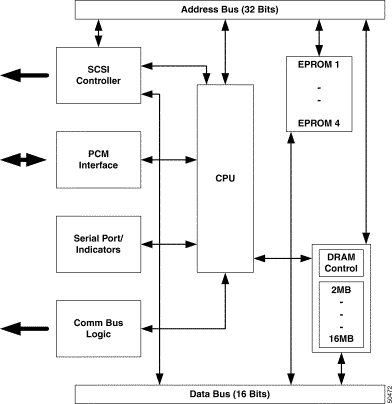
The IPRC contains a 68340-based Packet Processor that interfaces to the comm bus. A packet processor is part of all cards with the exception of the Network Bus Controller (NBC3).
The packet processor consists of the 68340 microcomputer, program and data memory, associated RAM, EPROM, and address decode circuitry, the comm bus interface, an asynchronous serial port, and the LED register. It is via the comm bus that the NBC issues commands to the IPRC in the form of data packets. The IPRC reports the status of its voice channels over the same bus using the data packet protocol. When polled by the NBC, the packet processor reports any status change. The 68340 provides the intelligence for the packet processor and, therefore, for the IPRC.
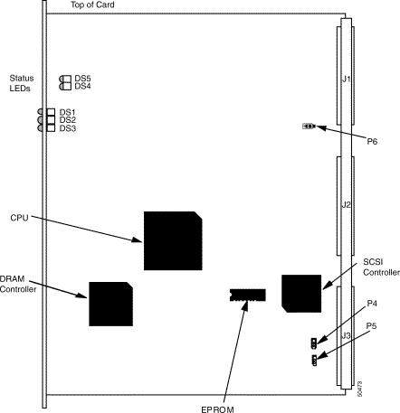
The packet processor supports a diagnostic serial port connected to a signal line on the backplane and also controls three status LEDs (red, yellow, and green) which are visible through the card's front panel.
The IPRC has three LEDs that are visible through the front panel and two additional internal LEDs that are not visible from the front panel.
A red, a yellow, and a green LED (DS1, DS2, and DS3, respectively) are visible through the IPRC's front panel to indicate the status of the card. Typically, an illuminated red LED indicates a major card failure, a yellow LED indicates a minor card failure, and a green LED indicates the card is in standby or diagnostic mode. Table 4-1 shows the card status information provided by the illuminated LEDs.
| Card Status | Green (DS3) | Yellow (DS2) | Red (DS1) |
|---|---|---|---|
Card Plugged In (not initialized) | On | On | On |
Self Test | On | Blinking | Off |
Receiving Download | Blinking | Off | Off |
Card Out Of Service (OOS) | On | Off | Off |
Standby/Diagnostic Mode | On | On | Off |
Major Alarm | Off | Off | On |
Minor Alarm | Off | On | Off |
Card Failure | On | Off | On |
The red LED inside the front panel (DS5) is tied to the HALT line on the 68340 CPU. DS5 is illuminated when the CPU stops processing.
The green LED inside the front panel (DS4) is the heartbeat indicator for the IPRC. During normal operation, DS4 flashes. Whenever the normal background operation is interrupted (for example, during memory testing), DS4 stops flashing at its last known illumination state.
The IPRC uses a SCSI interface to download prompt data to and from the system controller. The SCSI interface is maintained by an NCR 53C94 SCSI Controller, or equivalent, located at U3.
A 16-bit DMA interface is set up between the 68340 and the 53C94 to transfer data between the IPRC DRAM and the SCSI bus. This DMA interface physically exists on the data bus, but program control prevents other devices from using the data bus during DMA operations. The 68340 provides the DMA channel control through the on-chip DMA Module.
The IPRC cards connect to the system controller cards (side A and B) with ribbon cables on the rear of the midplane. One ribbon cable connects from the A-side connector on the small daughter board located on the lower, right side of the midplane as viewed from the rear. Another ribbon cable connects from the B-side connector. These connectors are clearly marked on the daughter board.
The other end of each ribbon cable has connectors for up to four IPRC cards. These are connected to the lower set of pins (J3) on the rear of the midplane for each IPRC installed. Pin 1 on the connector is identified by the red stripe on the ribbon cable. The connectors are installed with Pin 1 facing up.
|
Note Ensure that each cable connection on the rear of the midplane is aligned with a slot containing an IPRC card. |
This section describes the connectors and jacks on the IPRC.
|
Note J2 Pin Assignments are proprietary and are therefore not documented for customer use. |
Table 4-2 lists the pin assignments for J1 on the IPRC.
| Pin | Row A | Row B | Row C |
|---|---|---|---|
1 | DGND | Unused | DGND |
2 | DGND | Unused | DGND |
3 | DGND | Unused | DGND |
4 | DGND | Unused | DGND |
5 through 10 | Unused | Unused | Unused |
11 | Digital +5V | Unused | Digital +5V |
12 | Digital +5V | Unused | Digital +5V |
13 | Digital +5V | Unused | Digital +5V |
14 through 21 | Unused | Unused | Unused |
22 | Card Address Bit 1 | Unused | Card Address Bit 0 |
23 | Card Address Bit 3 | Unused | Card Address Bit 2 |
24 | Card Address Bit 5 | Unused | Card Address Bit 4 |
25 | Card Address Bit 7 | Unused | Card Address Bit 6 |
26 | SRV | Unused | Unused |
27 | DID | Unused | Unused |
28 | RST | Unused | Unused |
29 through 31 | Unused | Unused | Unused |
32 | DGND | Unused | DGND |
The IPRC uses the first 25 pins on J3 rows A and C for SCSI bus signals. Table 4-3 specifies the pin connections.
| Pin | Row A | Row B | Row C |
|---|---|---|---|
1 | SD0 | Unused | DGND |
2 | SD1 | Unused | DGND |
3 | SD2 | Unused | DGND |
4 | SD3 | Unused | DGND |
5 | SD4 | Unused | DGND |
6 | SD5 | Unused | DGND |
7 | SD6 | Unused | DGND |
8 | SD7 | Unused | DGND |
9 | SDP | Unused | DGND |
10 through 12 | DGND | Unused | DGND |
13 | TPWR | Unused | DGND |
14 | DGND | Unused | DGND |
15 | DGND | Unused | DGND |
16 | ATN | Unused | DGND |
17 | DGND | Unused | DGND |
18 | BSY | Unused | DGND |
19 | ACK | Unused | DGND |
20 | SRST | Unused | DGND |
21 | MSG | Unused | DGND |
22 | SEL | Unused | DGND |
23 | CD | Unused | DGND |
24 | REQ | Unused | DGND |
25 | 1O | Unused | DGND |
26 through 32 | Unused | Unused | Unused |
The IPRC has a front panel jack used to access internal diagnostics and internal debugger utilities, and to obtain run-time status/error messages. The front panel jack is an asynchronous serial port that is configured at 9600 baud, 8 bits, no parity. The front panel jack accepts the standard phone jack used on all system port cards.
The IPRC is manufactured by Cisco Systems, Inc. Jumper plugs are factory set for use in systems. Figure 4-3 and Figure 4-4 show the location of the factory set jumpers. Refer to the jumper settings to verify configuration jumper settings prior to installing the IPRC in a Port Subrack.
|
Note Artwork revision levels for individual printed circuit boards (PCBs) are etched on the solder side of the PCB near the front panel of each card. |
If a card is improperly configured, it may fail to operate. Be certain to verify configuration settings before installing a replacement service circuit card in the system.
The IPRC is provided with an EPROM in socket U2. The default jumper configuration of P4 and P5 for 1 Mb (128k x 8), is shown in Figure 4-3.

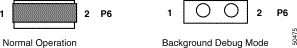
Jumper J6 is used to disconnect the Reset signal from the system backplane to the IPRC. Removal of this jumper prevents the NBC from resetting the IPRC. Remove this jumper only when using the background mode debugger on the IPRC on a system environment. During background mode debug operations, normal program execution on the 68340 is interrupted. Failure to remove this jumper during debugging results in the IPRC being reset as soon as the 68340 is placed in debug mode.
Figure 4-4 shows the jumper configuration for normal and background mode operation. The Normal Operation setting is the default.
When an IPRC is added to the system, it is defined with the physical number of ports. The 64 and 128 port IPRC configurations may also be configured to support less than the physical port capacity. This feature enables the user to configure the port density in 8-port increments through the IPRC Card Configuration screen. (Refer to the Cisco VCO/4K System Administrator's Guide for more information.) The screen processing frees up or reallocates time slots based on the defined port density.
The Subrate Switching Card (SSC) is a service circuit card that occupies a single card slot in the VCO/4K.
The SSC allows the VCO/4K system to switch voice and data calls at N x 8 kbps rates (where N equals the number of channels). With the SSC, service providers can improve trunk efficiency up to eight times by "packing" eight subrate channels within a traditional 64 kbps channel.
The SSC enables VCO/4K switches to be used as Base Station Controllers (BSCs) in wireless telephone networks or other networks that carry compressed audio.
You can remove or replace the SSC without shutting off the system.
The SSC supports a switching matrix of up to 2000 64-kbps time slots, allowing up to 16,000 8-kbps subrate connections.
Microprocessor: | (1) MC68360 |
Memory: | 1 MB DRAM |
| 128 KB EPROM |
Power Requirements: | 30 Watts @ 5 VDC max |
| .5 Watts @ 15 VDC |
| .5 Watts @ -15 VDC |
Redundant SSC operation requires that two SSC cards be present—an active card and a standby card. The standby card is responsible for verifying the operational status of the active card. When the standby card determines that the active card has failed, the standby card:
Subrate switching requires that both the active and standby SSCs be located in the same rack and on the same level.
The presence of an SSC does not affect system level redundancy.
The SSC controls the subrate switching matrix with one Motorola MC68360 QUICC (QUad Integrated Communications Controller).
The SSC includes the following circuitry:
The following list provides hardware configuration information for the SSC.
All configuration parameters for the SSC are configured in software through the administration interfaces. There are no hardware options that you can select on the SSC.
The application software, downloaded to the SSC, enables control and configuration of the card, as well as each subrate channel. For more information about configuring subrate service, refer to the Subrate Configuration screen in the Cisco VCO/4K System Administrator's Guide.
Figure 4-5 shows the layout of the SSC.
The Service Platform Card (SPC) provides the service resources element of the three critical system elements of the VCO/4K — system control, port interfaces, and service resources. The SPC allows any service resource function of the VCO/4K to be performed with this card as a base platform, given a minimum of one Service Resource Module (SRM) mezzanine card on the board to perform the service function(s). Mezzanine cards have the capability to perform more than one service function, and to perform these functions simultaneously.
Some other features of the SPC:
The SPC Card is in compliance with all applicable U.S. and international standards. Refer to Table 4-4.
| Category | Standard |
|---|---|
Safety | UL1459 CSA C22.2 EN-60950 IEC-950 |
EMI/EMC | FCC Part 15 (US/Canada) EN55022 (Europe) EN50082-1 (Europe) VCCI (Japan) |
PCB Manufacture | IPC |
Microprocessor | MPC860MHZP-50 |
Memory | 8 MB Flash |
Power Requirements | 5 Volts - 1.5A - board only, no SRMs (Max) |
5 Volts - 1.0A - each SRM (Max) | |
5 Volts - 5.5A - board with four SRMs (Max) |
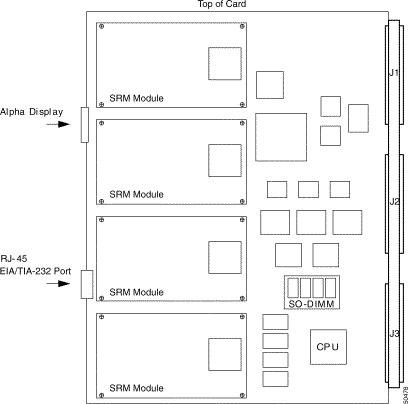
The SPC is a single-slot card. Up to four separate SRMs, mounted as mezzanine cards, provide processing resources.
The SPC is inserted in the VCO/4K switch from the front of the system.
The SPC contains the following elements:
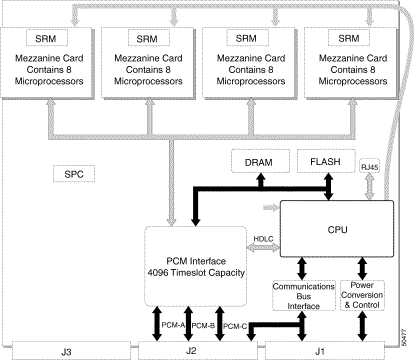
The block diagram for the SPC and SRM Modules is shown in Figure 4-6.
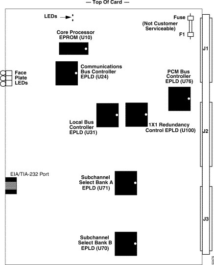
The SPC hardware layout is shown in Figure 4-7.
|
Note Not all components are shown. |
The processor and associated peripheral circuitry on the SPC is called the Core Processor. The Core Processor runs the card level application and diagnostics and is responsible for managing all SPC-based and mezzanine peripheral devices described in the sections that follow.
Features shown in Figure 4-6 are discussed in this section at a high level.
The Core Processor comprises the Motorola MPC860MHZP-50 CPU and associated peripherals and support circuitry. The main timing reference for the Core Processor is supplied by an on-board 3.3V crystal oscillator.
The SPC's architecture is dependent on a centralized (time division multiplexed and switched) HDLC controller connected to service engines (SEs) in a traditional multiprocessor star arrangement. In the SPC's particular implementation of this architecture, the HDLC controller is contained within the Core Processor. The PCM interface acts as the switching device, which spreads the communication time slots across the service engines. Refer to Figure 4-8.

The central processor is responsible for command and response message control of any service engine, or any combination of service engines. The use of HDLC in this star manner has several benefits for the SPC:
The Communications Processor Module within the MPC860MHZP-50 is internally routed to the time slot assigner. The transmit and receive data is routed through the TDMA interface to devices external to the MPC860MHZP-50. Once the data leaves the Core Processor, it has a time division multiplexed arrangement. This serial data is then routed to the PCM interface, where it is switched under the control of the Core Processor so the time slots are rerouted to the 32 service engine bound serial streams which contain regular PCM traffic. These 32 serial streams connect the service engines with the PCM interface.
The PCM interface routes 32 serial streams running at 4.096 Mbps each to the mezzanine card locations. Eight of the thirty-two streams are used by each mezzanine location. Each mezzanine card contains eight DSP Service Engines, each receiving one 4.096 Mbps, 64-time slot, serial, full duplex stream. One 64-kbps time slot from each stream is dedicated to the HDLC command/response data.
The SPC card displays status on a 5x7 alpha display located on the SPC front panel. Table 4-5 defines the alpha display states.
|
Note The SPC has a card failure LED immediately above the Alpha display. This LED indicates a major SPC circuit failure. If this is lighted, remove and reinsert the card. If the light illuminates again, replace the card. |
.
| Display | Meaning |
|---|---|
First Six Rows | |
SPC | Card is SPC |
Rotating line pattern | Download Progress Meter |
Bottom Row | |
1st LED (left) through the 4th LED (right) | Indicators for SRMs 1 through 4. A blinking LED indicates the associated SRM is configured. A constantly lighted LED indicates the SRM is populated but not configured. An unlighted LED indicates the SRM is not populated. |
5th LED (right) | Heartbeat indicator. Normal operation is one on/off cycle per second. Erratic cycle may indicate a card overload. A stopped cycle may indicate a card failure (reboot or replace). |
The communications bus is used by the Core Processor to communicate with the NBC. The communications bus interface protocol is managed by hardware-based state machines assisted by an interrupt-based CPU support mechanism.
Supported features include high-speed parallel communications to the NBC3 and Flash memory CPU-assisted download capability.
Each Service Resource Module (SRM) contains multiple service engines. Each engine consists of a single digital signal processor (DSP) and associated RAM. The design of the SRM ensures that each service engine is a totally independent entity. Up to four SRMs may be populated per SPC, with eight engines per SRM.
Each service engine is connected to the PCM serial highways (and the PCM interface) through the mezzanine interface. These PCM serial highways contain both PCM data and command/response HDLC traffic from the core processor.
A service engine incorporates a 16-bit, fixed-point, digital signal processor (DSP) and SRAM memory. This signal processing engine contains several interface mechanisms:
The mezzanine interface is based upon a TDM traffic switched HDLC command/response architecture (refer to the "HDLC-based multiprocessor Architecture" section), with status and control registers for proper identification and reset control over the mezzanine locations. Additionally, the mezzanine interface uses a serial boot mechanism as its sole core processor master-to-slave boot device.
The SRM core processor provides serial boot control of the mezzanine SRMs. A continuous serial stream of boot code is targeted at a single DSP or to a group of DSP service engines. Any individual DSP or group of DSPs may be booted simultaneously.
The SPC supports a variety of service facilities implemented via software. This application software executes on the SRM's DSPs. This allows the SPC to support multiple tone plans and easily updated algorithm changes.
The following services are provided:
The individual SEs operate independently. This results in the ability to:
The memory subsystem comprises components that interface to the Core Processor External Bus Interface. The Core Processor external bus consists of a 32-bit address bus, a 32-bit data bus, and several control signals to interface to a wide range of devices. This section discusses the configuration of the SPC's memory subsystem, which includes the FLASH and DRAM components.
The interface between the Core Processor and external devices uses control signals and a configurable memory controller contained within the MPC860MHZP-50.
DRAM is provided by 72-pin standard 32-bit wide Extended Data Out (EDO) 3.3V SO-DIMMs. SO-DIMM support is for multiple-bank 1 to 64-MB modules with a maximum of two banks per module.
Flash memory is the boot device. 8 MB of Flash are available for SPC and SE code to minimize boot-up time. The system controller can upgrade Flash memory without users having to remove the card because the Flash is hot-socketed.
The SPC PCM interface delivers up to 2016 time slots from the system backplane to service resources located on serial streams internal to the SPC. The PCM interface is a full duplex mechanism, capable of time-space-time switching on both the transmit and receive paths. Per time slot loopback is provided for diagnostic mechanisms. Non-bandwidth-impacting loopback is provided to facilitate algorithms.
There are three PCM buses on the VCO/4K backplane, known as the A, B, and C buses. The A and B buses are 8-bit parallel buses running at 8.192 MHz; the C-bus runs at 16.384 MHz. The C-bus is used with the ICC to achieve the extended port capacity of the VCO/4K.
The PCM interface performs the actual switching function. The interface routes 2016 full-duplex time slots to the mezzanine interface and consists of functionally separate transmit, receive, and NBI switch matrixes.
The interface is of the nonblocking time-space-time type and is completely controlled by the local core processor.
The power subsystem provides power to the on-board and mezzanine-based components on the SPC/SRM board pair, as well as protection from noise, overcurrent, and under and over voltage conditions. Alarming and voltage-monitored reset signals are provided to the core processor.
The power subsystem within the SPC mainboard is based upon two main functional components, the hot swap controller and the switching regulator. These components act together to protect the system from instantaneous current demands on any power rail that the SPC connects to, and additionally, to protect the SPC from dangerous events on the rails it depends upon.
The SPC is software configurable via downloads and Flash only. There are no jumpers, sockets, or replaceable PROMs on the SPC.
|
Note An SRM that is configured in the database but is not physically installed will appear in the M (maintenance) state rather than the O (OOS) state. |
Follow the directions in "VCO/4K Card Overview" to remove or replace an SPC.
To remove an SRM:
 |
Caution Make sure you observe proper ESD procedures when handling this card. Have a wrist strap in place before replacing the card. |
Step 2 Using a screwdriver, remove the four screws holding the SRM in place (one at each corner). Ensure all hardware, including washers, is retained.
Step 3 Gently remove the SRM, grasping it by the edges.
Step 4 Replace the screws and washers on the SPC for future use.
Step 5 Replace the SPC card in the system.
To add an SRM:
|
Caution Make sure you observe proper ESD procedures when handling this card. Have a wrist strap in place before replacing the card. |
Step 2 Using a screwdriver, remove the four screws and washers in the empty SRM location.
Step 3 Gently insert the SRM on the two connectors. Be careful not to bend the board as you insert it. The large, square Altera component should face the back (connector side) of the SPC (refer to Figure 4-7). (The SRM is keyed to prevent improper insertion.)
|
Caution Do not press on semiconductor devices. Pressing above connectors, firmly snap in one and then the other connector. Hand tighten with screwdriver. |
Step 4 Secure the SRM (refer to Figure 4-9) with the four screws and washers removed in Step 2.

Step 5 Replace the SPC card in the system.
![]()
![]()
![]()
![]()
![]()
![]()
![]()
![]()
Posted: Mon Aug 6 14:31:17 PDT 2001
All contents are Copyright © 1992--2001 Cisco Systems, Inc. All rights reserved.
Important Notices and Privacy Statement.