|
|

The Drop and Insert (D+I) card provides DS0 transmission-only access to the VCO/4K system. It supports a maximum of eight interfaces per card, synchronous operation at either 56 KB or 64 KB. The D+I card is configurable as DCE or DTE with normal or reverse bit-packing, and supports both EIA/TIA-449 and V.35 signal specifications for dates and clock leads only. The D+I card can be inserted into the system while the system is active.
Administration of the card is performed through the existing system administration console. Configuration messages are sent to the card from the system software through the NBC/NBC3 interface.
Microprocessor: | 68360 (25 MHz) |
Memory: | 4 MB DRAM |
| 256 KB EPROM |
Power Requirements: | +5 Volts 4 amps |
| -15 Volts 0.5 amps |
I/O Port Specifications: |
|
Input Level: | EIA/TIA-449 or V.35 (date and clock only) |
Output Level: | EIA/TIA-449 or V.35 (date and clock only) |
 |
Note The DB-9 to DB-37 cable for DCE operation can be ordered from Cisco Systems. |
Figure 3-1 shows a block diagram of the D+I card. The major elements of the card are:
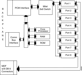
The core processor controls the eight synchronous serial links and communicates to the Network Bus Controller (NBC3) via the comm bus. The comm bus interface handshakes all signals with the NBC3, and moves data to and from memory through dedicated DMA channels present on the core CPU.
Each D+I port is connected to the Mitel 8985 voice/data switch. The Mitel switch switches data packets between multiple serial PCM highways generated within the PCM interface.
The core processor is a Motorola MC68360, a highly integrated microprocessor that can implement most of the core processor requirements through on-chip peripherals. The 68360 operates at 25 MHz.
The core processor has an EIA/TIA-232 port that is accessible from the face plate via an RJ-45 jack. The electrical signals are +12V and -12V (EIA/TIA-232).
The VCO/4K uses the PCM bus to move voice and data traffic between port cards. The NBC/NBC3 supplies clocking.
The PCM interface controls the following:
The core processor communicates with the NBC/NBC3 through the comm bus interface, which is implemented with the two DMA channels provided on the MC68360. One channel is dedicated to moving data off the comm bus, and one channel is dedicated to placing data on the comm bus.
The D+I card contains eight synchronous ports that can be individually configured by the system administrator. Because each D+I port interfaces to the VCO/4K, modem control signals are not provided. Only transmit and receive, clock and data signals are provided.
Users may select from the following features and configure the card on a per port basis:
Each D+I port is capable of operating at either 64 kbps or 56 kbps. The user selects the operating rate through system administration screens. Refer to the Cisco VCO/4K System Administrator's Guide for information on the D+I screens.
Each D+I port communicates over either an EIA/TIA-449 or V.35 link (designed for transmission only). Refer to Figure 3-2 for the appropriate wiring for the link.
On the port side, the cable connects via a 9-pin D-sub connector. On the equipment side, the cable connection is customer supplied and is dependent on the type of link. The cable pinouts for the D+I in DTE or DCE mode are different. Specific cables are required for each type of link.
If you are cabling the D+I card to the VCO/4K integrated SS7 system, note that a DB-9 to DB-37 cable is available from Cisco.
Each D+I port is individually capable of operating as either a DCE or DTE, as selected by the system administrator. When configured for DCE operation, the port uses the system clock to create the transmit and receive clocks. In DCE mode, the transmit and receive data path is not subject to data slips. This is the preferred configuration.
When configured for DTE operation, the port uses the received clocks to transmit data as well as receive data. Because receive clocks may not be locked to the VCO/4K system clock, the transmit and receive data paths are subject to data slips. In DTE mode, the port may lose its transmit and receive clocks. (Refer to the Cisco VCO/4K System Administrator's Guide for information on selecting DCE or DTE operation.)
Each port has a transmit and receive loss of clock (LOC) detector. When a port is in DTE mode and an LOC occurs, or an LOC condition clears, the core processor is informed via an interrupt. When a port is in DCE mode, no LOC events occur.
Each port has the following signals:
|
Note The D+I card cannot be used as a system clock reference source. |
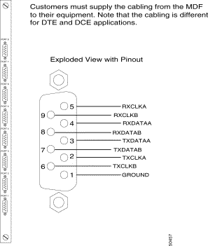
The D+I port only operates in a synchronous mode and as such, only the Data and Clock signals are provided. All I/O signals exit the board through the J3 connector, and an MDF board provides the interface to eight DB-9 female connectors. The eight female DB-9 connectors provide the necessary signals for EIA/TIA-449/V.35 connection.
The DB-9 pinout is shown in Table 3-1.
| Ground | Pin 1 | GND |
|---|---|---|
Transmit Clock A | Pin 2 | TXCLKA |
Transmit Clock B | Pin 6 | TXCLKB |
Transmit Data A | Pin 3 | TXDATAA |
Transmit Data B | Pin 7 | TXDATAB |
Receive Clock A | Pin 5 | RXCLKA |
Receive Clock B | Pin 9 | RXCLKB |
Receive Data A | Pin 4 | RXDATAA |
Receive Data B | Pin 8 | RXDATAB |
Figure 3-2 illustrates the DB-9 pinout.
.
Users may select normal or reverse bit ordering. The bits may be packed into a PCM byte in normal or reverse order as shown in Table 3-2.
| Mode | Bit 7 MSB | Bit 6 | Bit 5 | Bit 4 | Bit 3 | Bit 2 | Bit 1 | Bit 0 LSB |
|---|---|---|---|---|---|---|---|---|
64 kbps Normal | 1st bit | 2nd bit | 3rd bit | 4th bit | 5th bit | 6th bit | 7th bit | 8th bit |
56 kbps Normal | 1st bit | 2nd bit | 3rd bit | 4th bit | 5th bit | 6th bit | 7th bit | Fixed at 0 |
64 kbps Reverse | 8th bit | 7th bit | 6th bit | 5th bit | 4th bit | 3rd bit | 2nd bit | 1st bit |
56 kbps Reverse | 7th bit | 6th bit | 5th bit | 4th bit | 3rd bit | 2nd bit | 1st bit | Fixed at 0 |
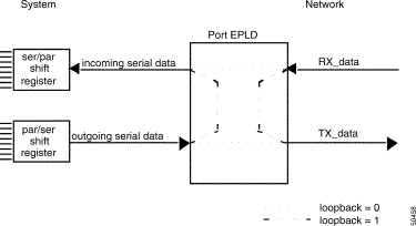
Each D+I port is capable of looping back the data presented at each interface. When you place a port in loopback, the data received at the port is looped back to the port transmit path without going through the FIFOs or slip circuits. Loopback also enables transmit data from the transmit PCM bus to go through the (Mitel) voice/data switch to the port controller EPLD, back through the voice/data switch, to the receive PCM bus.
The port EPLD provides all clock selection and synchronization, control of the port side of the FIFOs, error detection, and loopback. All input signals to the EPLD are synchronized with the internal 8 MHz clock so that the state machines are synchronous.
The Rx and Tx data is sent directly from the port interface, and the incoming and outgoing serial data goes to the shift registers prior to the FIFOs.
.
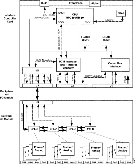
The Interface Controller Card (ICC) is a high-capacity network interface engine. The ICC employs a midplane architecture which enables it to connect with a series of I/O modules specific to different network interface requirements. The midplane isolates the unique physical characteristics of each type of connection leaving the ICC to perform all of the signaling and protocol processing independently. There are six I/O modules supporting 4, 8, or 16 network spans. A C-bus enabled, VCO switching platform (VCO/4K Series) with a full complement of ICCs and 16-span I/O modules will support more than 4000 ports.
For information on the I/O modules, refer to the "Interface Controller Card T1 I/O Module" section, or the "Interface Controller Card E1 I/O Module" section, depending on your network requirements.
The ICC is fully programmable, enabling user control over individual channels.
Other features:
Restrictions:
The ICC is in compliance with all applicable U.S. and international standards. See Table 3-3.
| Category | Standard |
|---|---|
Safety | UL1459 CSA C22.2 EN-60950 IEC-950 |
EMI/EMC | FCC Part 15 (US/Canada) EN55022 (Europe) EN50082-1 (Europe) VCCI (Japan) |
PCB Manufacture | IPC |
Microprocessor | MPC860MH-50 |
Memory | 8 MB Flash, 16 MB DRAM SIMM |
Power Requirements | 5 Volts - 3.5A (Typical) |
The ICC is a single-slot card. A separate I/O module provides access to the network interfaces. The I/O module includes active circuitry such as T1/E1 framers and is unique to each network configuration. Regardless of the span configuration, the CPU card is common.
The ICC is inserted in the VCO/4K from the front of the system. An I/O Module, inserted at the rear of the system, aligns with each ICC.
The ICC contains the following functions:
The block diagram for the ICC and I/O Module is shown in Figure 3-4.

The Core Processor coordinates all activities of the ICC including:
The MPC860 processor controls up to 16 network trunks and manages all aspects of the network interface such as framing, call control, mu-law/a-law conversion, gain control, etc.
The MPC860 processor communicates to the Network Bus Controller (NBC) via the comm bus. The comm bus interface is controlled primarily by dedicated hardware. The comm bus interface handshakes all signals with the NBC and retrieves data from, and stores data to memory, by interrupting the MPC860 at the end of a cycle.
The MPC860 Processor has one EIA/TIA-232 port, which is accessible from the face plate. This port utilizes an RJ-45 jack. The electrical signal levels are EIA/TIA-232 compliant.
|
Note The front panel RJ-45 jack is not intended for customer use. |
The Flash memory boots the processor so that the application and/or diagnostic software can be downloaded over the comm bus when new revisions are required. The boot Flash is 8 MB.
The MPC860 processor has an EDO DRAM array of 16 MB on a 72-pin SIMM memory device (similar to a PC memory). The EDO DRAM array is arranged in a 32-bit arrangement, and is controlled by the on-chip DRAM controller provided by the MPC860.
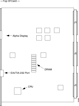
The ICC displays status on a 5x7 Alpha display located on the ICC front panel. Table 3-4 defines the Alpha display states.
|
Note The ICC has a card failure LED immediately above the Alpha display. This LED indicates a major ICC or I/O card circuit failure. Replace the cards if this is lighted. |
| Display | Meaning |
|---|---|
B | Blue Alarm |
D | D-channel failure |
E1 | Card is E1 |
F | Framing Error |
M | Maintenance |
N | No I/O Module |
O | Out-of-Service |
R | Red Alarm |
T1 | Card is T1 |
Y | Yellow Alarm |
Download Progress Meter | Rotating line pattern |
Only the most severe alarm state is displayed on the LED.
The bottom row of the LED matrix identifies which group of spans is reporting the alarm. The leftmost LED indicates group 1, the next LED indicates group 2, etc. The fifth, right most, LED indicates the state of the core processor. If this fifth LED stops blinking, the card should be removed and reinserted. If the LED still fails to blink, replace the card.
Table 3-5 lists the conditions that cause a major or minor alarm in the ICC.
| Major Alarm | Minor Alarm |
|---|---|
Loss of Carrier | Slip Threshold Exceeded |
OOF Threshold Exceeded | |
Loss of Remote Carrier | |
Signaling Bit Error | |
OOF Error | |
Out-of-Service (OOS) |
The MPC860 processor uses the comm bus to communicate with the NBC. The comm bus Interface protocol is managed mostly by hardware, although CPU control is required. An EPLD controls the handshaking and read/write strobes to two FIFOs which store inbound and outbound packets.
The communications bus has the following associated functions:
The comm bus is a one-byte-wide half-duplex interface. This interface facilitates the transfer of messages between the port cards and the NBC3.
The comm bus architecture of the ICC is responsible for:
The comm bus architecture supports directed downloads.
There are three PCM buses on the Cisco Systems backplane, known as the A, B, and C Buses. These are 8-bit parallel buses running at 8.192 MHz, with the exception of the C-bus which runs at 16.384 MHz. The C-bus is used with the ICC to achieve 4K ports.
Each inbound and outbound timeslot has the ability to apply mu-law/a-law conversion and gain control. The gain/law conversion occurs between the SMX-controlled Transmit PCM DPRAMs and the Transmit PAC.
The available gains are: 0 dB, -3 dB, -6 dB, -12 dB, +1.5 dB, +3 dB, +6 dB, and +12 dB.
The J3 connector is the interface between the I/O Module and the ICC. This includes the following: functions:
You download the application software to each span controller, enabling independent provisioning of each span as well as each channel.
The ICC supports a number of programmable parameters which allow card customization:
Cisco can assist in creating your parameters on a floppy disk which you load into the VCO.
Support for network protocols is provided by a state machine (the Protocol State machine) that operates on the ICC. This is a software module that defines how the ICC will behave as a result of specific events.
The state machine performs an action for each predefined event. This state machine is fully programmable, allowing any action to take place as a result of any specific event. This allows predefined configuration of a port or span. Standard network (T1, E1) protocols are preprogrammed. The standard protocols may be modified to meet specific needs and saved as a customized protocol or a new protocol can be developed. All protocols (preprogrammed, modified, or newly developed) are stored with a unique identifier.
To configure the ICC with a new protocol, select one or more ports/spans on which the protocol will be executed. The protocol configuration information is transmitted to the ICC when each span is activated.
A standard or user-defined protocol is implemented at the port level when the ICC is configured as a T1 card and implemented at the span level when configured as an E1 card. Also, to configure the port (T1) or span (E1) with any protocol, the port or span cannot have active calls. The port or span must be placed in the OOS state when changing protocol configuration.
The ICC is software configurable via downloads. There are no jumpers or replaceable PROMs on the ICC.
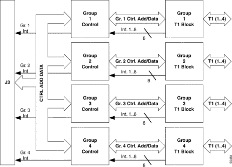
The VCO/4K uses active I/O modules in conjunction with the ICC to connect to the network. Each I/O Module uses one slot on the backplane and supports one ICC. The I/O Module is located at the back of the switch and must be aligned with the ICC. A block diagram for the ICC I/O Module is shown at the bottom of Figure 3-6.
The T1 I/O Module is a specialized backplane card that provides T1 network connection to the ICC. It is available in three configurations supporting 4, 8, or 16 T1 spans. The ICC is inserted in the VCO switch from the front of the system. The I/O Module, inserted at the rear of the system (before ICC insertion), aligns with each ICC.
The T1 I/O module supports a 100-ohm network interface and includes active circuitry such as T1 framers.
For information on the ICC, refer to the "Interface Controller Card (ICC)" section.
The ICC I/O Module is in compliance with all applicable U.S. and international standards. See Table 3-6.
| Category | Standard |
|---|---|
Safety | UL1459 CSA C22.2 |
Jitter | Pub 62411 |
EMI/EMC | FCC Part 15 (US/Canada) VCCI (Japan) |
PCB Manufacture | IPC |
Lightning/Power Cross | CSA C22.2 FCC Part 68 CS-03 |
Telecom | FCC Part 68 CS-03 JATE AT&T Publication 62411 Bellcore PUB43801 TR-NPL-000054 TR-TSY-000510 TR-TSY-000191 ANSI T1.403 |
Power Requirements | 5 Volts (from the ICC) 4 Span T1 - 1.16A 8 Span T1 - 1.42A 16 Span T1 - 1.95A |

|
Note Not all components are shown. |
Table 3-7 and Table 3-8 list the pinouts for the RJ-45 female receptacles on the I/O module. Use these tables as a reference when you wire RJ-45 male connectors to cables at the installation site.
Table 3-7 lists the external interface for the I/O Module to the network. Table 3-8 lists the external interface for the I/O Module to the Cisco AS5300. Figure 3-8 shows the pin orientation for the RJ-45 connector.
| VCO Side | Network Side |
|---|---|
Pin 1 Tx Ring | Network Rx Ring |
Pin 8 Tx Tip | Network Rx Tip |
Pin 4 Rx Ring | Network Tx Ring |
Pin 5 Rx Tip | Network Tx Tip |
| VCO Side | AS5300 Side |
|---|---|
Pin 1 Tx Ring | Pin 1 Rx Ring |
Pin 8 Tx Tip | Pin 2 Rx Tip |
Pin 4 Rx Ring | Pin 4 Tx Ring |
Pin 5 Rx Tip | Pin 5 Tx Tip |

You download the application software to each span controller, enabling independent provisioning of each span as well as each channel.
The ICC supports a number of programmable parameters which allow card customization:
Cisco can assist in creating your parameters on a floppy disk which you load into the VCO/4K.
The J3 connector is the interface between the I/O Module and the ICC. This includes the following functions:
The I/O Module interfaces the VCO/4K system with 4, 8, or 16 T1 digital data carrier streams. Each stream consists of a 1.544-Mbps, 24-channel, bipolar digital data stream. VCO system synchronization may be set to the receive clock of any T1 span on the I/O Module (the Master Timing Link).
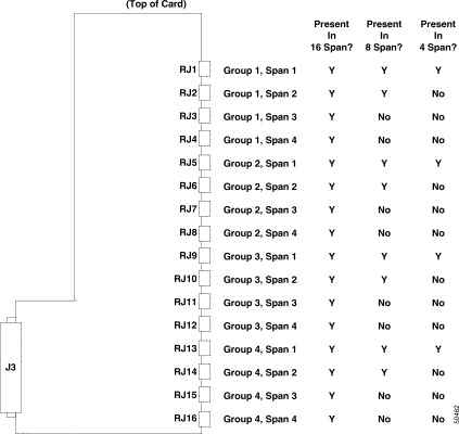
The I/O module's framers are segmented into groups of four called Framer Groups. This design approach reduces the chance of a single point of failure on the card. A hardware failure on the I/O Module normally affects only a group (1, 2 or 4 spans) and not the entire I/O Module. Figure 3-9 illustrates the span grouping architecture of the I/O Module.
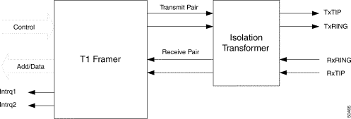
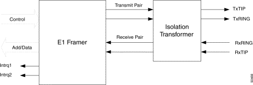
The T1 framer (Figure 3-10) contains a Line Interface Unit (LIU). The LIU contains three sections: 1) the receiver which handles clock and data recovery, 2) the transmitter which wave shapes and drives the T1 line, and 3) the jitter attenuator.
The LIU adjusts to the T1 signal being received and can handle T1 transmit line lengths from 0 to 655 feet as configured from the Port Configuration screen (See the Cisco VCO/4K System Administrator's Guide).
Circuitry on the I/O card detects loss of carrier errors, framing errors, and remote alarms on its incoming T1 stream. It also detects receive/transmit slips which occur when the rate at which data is sent on the incoming stream is different from the rate at which data is transmitted onto a PCM data bus, or when data from the PCM data bus is transmitted at a different rate, such as in loop-timed configurations. The ICC contains elastic PCM data buffers to minimize slips caused the T1 stream frequency jitter.
Table 3-9 details the T1 I/O Module's input and output stream specifications.
.
Input Stream | |
Format | D3/D4 or ESF |
Data transparency | Alternate Mark Inversion (AMI), Bipolar with 8 zero substitution (B8ZS), Bit 7 zero stuff, none. |
Frequency | 1.544 Mbps +/- 76 bps |
Impedance | 100 ohms |
Output Stream | |
Format | D3/D4 or ESF |
Data transparency | Alternate Mark Inversion (AMI), Bipolar with 8 zero substitution (B8ZS), Bit 7 zero stuff, none. |
Line Equalization (Drive) | 0 to 655 ft |
Frequency | 1.544 Mbps +/- 76 bps |
Impedance | 100 ohms |
The combined framer/LIU performs the following functions:
|
Note You can use B8ZS for T1 to maintain 1s density (and timing) while providing data transparency. |
There are no jumpers or replaceable PROMs on the I/O Module.
The VCO/4K uses active I/O modules in conjunction with the ICC to connect to the network. Each I/O Module uses one slot on the backplane and supports one ICC. The I/O Module is located at the back of the switch and must be aligned with the ICC. A block diagram for the ICC I/O Module is shown at the bottom of Figure 3-11.
The E1 I/O Module is a specialized backplane card that provides E1 network connection to the ICC. It is available in three configurations supporting 4, 8, or 16 E1 spans. The ICC is inserted in the VCO/4K switch from the front of the system. The I/O Module, inserted at the rear of the system (before ICC insertion), aligns with each ICC.
The E1 I/O module supports a 120-ohm network interface for E1 and includes active circuitry such as E1 framers.
|
Note The E1 I/O Module also supports a 75-ohm network interface when optional Balun impedance matching devices are used. |
For information on the ICC, refer to the "Interface Controller Card (ICC)" section.
The ICC I/O Module is in compliance with all applicable U.S. and international standards. See Table 3-10.
Power Requirements | 5 Volts (from the ICC) 4 Span E1 - 1.16A 8 Span E1 - 1.42A 16 Span E1 - 1.95A |
|
Note Not all components are shown. |
Table 3-7 and Table 3-8 list the pinouts for the RJ-45 female receptacles on the I/O module. Use these tables as a reference when you wire RJ-45 male connectors to cables at the installation site.
Table 3-7 lists the external interface for the I/O Module to the network. Table 3-8 lists the external interface for the I/O Module to the Cisco AS5300. Figure 3-13 shows the pin orientation for the RJ-45 connector
| VCO Side | Network Side |
|---|---|
Pin 1 Tx Ring | Network Rx Ring |
Pin 8 Tx Tip | Network Rx Tip |
Pin 4 Rx Ring | Network Tx Ring |
Pin 5 Rx Tip | Network Tx Tip |
| VCO Side | AS5300 Side |
|---|---|
Pin 1 Tx Ring | Pin 1 Rx Ring |
Pin 8 Tx Tip | Pin 2 Rx Tip |
Pin 4 Rx Ring | Pin 4 Tx Ring |
Pin 5 Rx Tip | Pin 5 Tx Tip |
You download the application software to each span controller, enabling independent provisioning of each span as well as each channel.
The ICC supports a number of programmable parameters which allow card customization:
Cisco can assist in creating your parameters on a floppy disk which you load into the VCO/4K.
The J3 connector is the interface between the I/O Module and the ICC. This includes the following functions:
The E1 I/O module supports a 120-ohm network interface for E1.
|
Note The E1 I/O Module also supports a 75-ohm network interface when optional Balun impedance matching devices are used. (See Technical Bulletin # 63102750100.) |
The I/O Module interfaces the VCO/4K system with 4, 8, or 16 E1 digital data carrier streams. Each stream consists of a 2.048-Mbps, 32-channel, bipolar digital data stream (E1). VCO/4K system synchronization may be set to the receive clock of any E1 span on the I/O Module (the Master Timing Link).
The I/O module framers are segmented into groups of four called Framer Groups. This design approach reduces the chance of a single point of failure on the card. A hardware failure on the I/O Module normally affects only a group (1, 2 or 4 spans) and not the entire I/O Module. Figure 3-14 illustrates the span grouping architecture of the I/O Module.
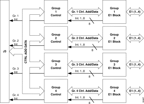
The E1 framer (Figure 3-15) contains a Line Interface Unit (LIU). The LIU contains three sections: 1) the receiver which handles clock and data recovery, 2) the transmitter which wave shapes and drives the E1 line, and 3) the jitter attenuator.
The LIU adjusts to the E1 signal being received and can handle E1 transmit line lengths to 1.5 km as configured from the Port Configuration screen (see the Cisco VCO/4K System Administrator's Guide).
Circuitry on the I/O card detects loss of carrier errors, framing errors, and remote alarms on its incoming E1 stream. It also detects receive/transmit slips which occur when the rate at which data is sent on the incoming stream is different from the rate at which data is transmitted onto a PCM data bus, or when data from the PCM data bus is transmitted at a different rate, such as in loop-timed configurations. The ICC contains elastic PCM data buffers to minimize slips caused the E1 stream frequency jitter.
Table 3-13 details the E1 I/O Module's input and output stream specifications.
Input Stream | |
Format | CAS, Clear Channel, or NET5 ISDN |
Data transparency | Alternate Mark Inversion (AMI), Bipolar with 8 zero substitution (B8ZS), Bit 7 zero stuff, none. |
Frequency | 2.048 Mbps +/- 50bps |
Impedance | 120 ohms +/- 10% |
Output Stream | |
Format | CAS, Clear Channel, or NET5 ISDN |
Data transparency | Alternate Mark Inversion (AMI), Bipolar with 8 zero substitution (B8ZS), Bit 7 zero stuff, none. |
Line Equalization (Drive) | CCITT G.703 |
Frequency | 2.048 Mbps +/- 50bps |
Impedance | 120 ohms +/- 10% |
The combined framer/LIU performs:
|
Note You can use HDB3 for E1 to maintain (1s) density (and timing) while providing data transparency. |
There are no jumpers or replaceable PROMs on the I/O Module.
![]()
![]()
![]()
![]()
![]()
![]()
![]()
![]()
Posted: Mon Aug 6 14:21:31 PDT 2001
All contents are Copyright © 1992--2001 Cisco Systems, Inc. All rights reserved.
Important Notices and Privacy Statement.