|
|

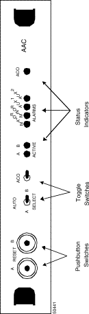
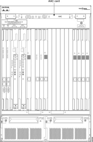
The Alarm Arbiter Card (AAC) is the central control point for system resets and alarm indication. The AAC is mounted at the top of the VCO/4K as shown in Figure 2-1. Switches on the front panel enable system controller resets and select which system controller is to be master. Status LEDs indicate the currently enabled system controller and major/minor alarms.
The AAC is attached to the Alarm Interface Card (AIC). The AIC accepts fault signals from the VCO/4K Power Subsystem, Fan Unit, and Ring Generator, and generates a single fault signal to the AAC. The AIC also conditions the fault signals for the AAC. Figure 2-2 shows the location of the AAC and AIC.
In VCO/4K applications, the host computer can set any of the alarms by software command. The VCO/4K may also support components which feature programmable alarm severity.
For a complete listing of system alarms supported by Generic software, refer to the Cisco VCO/4K System Administrator's Guide.

Watchdog Timer Parameters: |
| |
| After Reset/Power up: | 5 - 7 minutes |
| Normal operation: | 5 - 10 seconds |
Alarm Types: |
|
|
| MAJOR, MINOR, AUX 1, AUX 2 | |
| Visual indicators on AAC front panel | |
| External NO and NC relay contacts provided for each alarm | |
External Contacts | Type = 2 Form C |
|
| Rating = 0.5A @ 24 VDC, 0.25A @ 120VAC (Resistive load only) | |
Power Requirements: | +12 VDC | @ 1A |
Physical Dimensions | Height: | 6.3 in. (160 mm) |
| Width: | 9.2 in. (234 mm) |
| Depth: | 0.631 in. (16 mm) |
Power Requirements: | +5 VDC @ 0.2A (redundant) |
|
Physical Dimensions | Height: | 2.75 in. (70 mm) |
| Width: | 14.75 in. (374 mm) |
| Depth | .0631 in. (16 mm) |
The AAC is the hardware interface point for manual and automatic bus resets and alarms. It also functions as a control point for the selection of system controllers in systems equipped with redundant control. Power reset and watchdog timer circuitry is duplicated for A-side and B-side system controllers in VCO/4K systems to minimize possible system effects of AAC failures. Figure 2-3 is a simplified block diagram of the AAC.
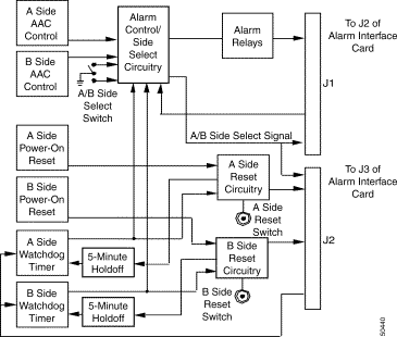
The watchdog timer for a particular system controller is disabled for approximately 5 minutes after that side is reset with the AAC. The watchdog timer is also disabled for a particular controller side if the other system controller is selected with the SELECT switch on the AAC front panel.
The AAC monitors the status of both system controllers and switches active controllers if one of the following conditions occurs:
For the switchover to occur, the following conditions must be true:
It may take up to one second for the actual switchover to occur. Use the front panel SELECT switch to immediately force a switchover, regardless of the state of the Standby controller. However, make sure you use this type of switchover only in an emergency; database sanity checks are not performed.
 |
Note Cisco Systems strongly recommends using the Maintenance Menu to force a switchover. Refer to the Cisco VCO/4K System Administrator's Guide for more information. |
On the left side of the front panel are two push-button switches labeled RESET A and RESET B (refer to Figure 2-4 ). Press RESET A to reinitialize the A-side (left) controller; press RESET B to reinitialize the B-side (right) controller.
The SELECT switch is a three-position toggle switch that determines which controller in a redundant control system is currently active. The AUTO setting works for nonredundant and redundant control systems. In nonredundant control systems, the A-side is always active. SELECT A makes the system controller on the left (front view) active; SELECT B makes the right system controller active.
Manually selecting one side disables the watchdog timer of the other side. However, if the manually selected controller should fail, automatic switchover will not be performed. With redundant control systems, always return the SELECT switch to the AUTO position after manually selecting A-side. When a redundant system powers up, the AAC uses Side A as the active controller (if operational) when the switch is set to AUTO.
|
Note In a redundant system in which the A-side is powered off and the system is to be brought up with the B-side active, the AAC switch must be set to SELECT B. If the AAC switch is in AUTO, the system will come up in Standby. |
The Alarm Cut-Off (ACO) switch is disabled. Changing the ACO switch has no effect on the audible alarm.
Two green LEDs labeled ACTIVE indicate whether the A-side or B-side system controller is currently the master. Only one of these LEDs is illuminated during normal system operation. The active system controller is also indicated on the bottom message line of the master console display screen.
A red LED illuminates when a MAJOR alarm is signaled by hardware or software. Yellow LEDs indicate MINOR and AUX 1 or AUX 2 alarms. MAJOR and AUX 1 LEDs illuminate when a Power Subsystem or Fan Unit failure occurs. A separate yellow LED illuminates when ACO is enabled.
|
Note Alarm LEDs on the AAC are disabled when the Audible Cutoff option on the System Alarms Display administration screen is chosen from the Maintenance menu. Refer to the Cisco VCO/4K System Administrator's Guide for more information on this option. |
Refer to the Cisco VCO/4K System Maintenance Manual for more information on alarm LEDs.
The AAC autonomously sets MAJOR, MINOR, and AUX 1 alarms based on the following criteria:
The J1 connector carries the signals related to one of four peripheral functions to the External Alarms terminal strip, automatic A/B transfer switches, or the Power Subsystem. Table 2-1 lists the pin assignments for the J1 connector.
The J1 connector is attached to connectors JP1, JP3, JP4, and JP5 of the AIC, which provides routing for the signals to and from the AAC.
The J2 connector plugs into the AIC J3 connector. The AAC receives alarm commands from the active system controller, and the watchdog timer "kicks" from both system controllers via the J2 connector. The signals at J2 are proprietary and, therefore, no listing of pin assignments is provided.
The AAC derives power from J2. At least one Combined Controller Assembly must be installed and powered up for the AAC to power up.
| Pin | Signal | Pin | Signal |
|---|---|---|---|
SLOT 1 - External Alarms | |||
1 | Unused | 33 | Unused |
2 | Major Alarm COM | 34 | Major Alarm CLSD |
3 | Major Alarm COM | 35 | Major Alarm OPEN |
4 | Minor Alarm COM | 36 | Minor Alarm CLSD |
5 | Minor Alarm COM | 37 | Minor Alarm OPEN |
6 | AUX 1 Alarm CLSD | 38 | AUX 1 Alarm COM |
7 | AUX 1 Alarm OPEN | 39 | AUX 2 Alarm COM |
8 | AUX 2 Alarm CLSD | 40 | AUX 2 Alarm OPEN |
SLOT 2 - A/B Transfer Switch | |||
9 | Unused | 41 | Unused |
10 | Side Select | 42 | Reserved |
11 | Reserved | 43 | DGND |
12 | Reserved | 44 | DGND |
13 | Reserved | 45 | DGND |
14 | Reserved | 46 | DGND |
15 | Reserved | 47 | DGND |
16 | Reserved | 48 | DGND |
SLOT 3 - Power Subsystem | |||
PROPRIETARY | |||
SLOT 4 - Backplane | |||
PROPRIETARY | |||
The J1 and J2 connectors of the AAC are mated to the J2 and J3 connectors of the AIC. The AIC cables are locked on to the connectors. The J2 connector is a 64-pin DIN connector.
The J2 connector breaks out the AAC signals into four connectors: JP1, JP3, JP4, and JP5. Table 2-2 lists the AAC signals for these connectors.
| Connector | Alarm |
|---|---|
JP1 | Backplane Alarms |
JP3 | Remote Alarm Output |
JP4 | A-B Switch for Peripherals |
JP5 | Selects Active NBC3 |
The J1 connector is for the Fan Alarm Input. It connects to the Fan Unit through the Fan Unit J4 connector.
Table 2-3 lists the electrical characteristics of the fault-indicator input to the AIC. The AIC combines and conditions the signals for input to the AAC.
| Signal | Voltage | Reference Voltage |
|---|---|---|
DC FAIL - Input Power | +0.5 to +5.0V | DC ground |
DC FAIL - Power | +0.5 to +5.0V | DC ground |
DC OK - Fan | +2.5 to +5.0V | DC ground |
DC OK - Ring Generator | 100 VAC | -48 VDC |
DC OK - Out | +0.5 to +3.0V | DC ground |
Figure 2-5 is a simplified block diagram of the AIC.
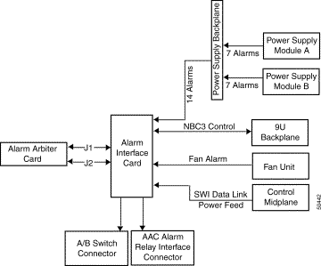
The output signals from the AAC are used to control remote functions. These signals are not modified by the AIC and are transferred directly from the AAC J1 connector to the AIC JP3 connector.
The DC OK signal on J1-10C is the merged signal of all incoming faults (PWR, FAN, and RING).
Figure 2-6 shows the location and correct installation of jumper plugs on the AAC.
Jumper location J3 allows you to selectively enable the on-board audible alarm device to sound for all alarm conditions or for major alarms only. The Alarm Cut-Off (ACO) switch is disabled. Changing the ACO switch has no effect on the audible alarm.
Position the jumper plug at J4 near R31 for all applications.
Figure 2-7 shows the location and labeling of the cable connections on the AIC.

The following subsections provide instructions for removing and replacing alarm arbiter and alarm interface cards.
 |
Caution Removing and replacing the AAC or AIC causes the system controller(s) to reset. Calls in progress will be lost and the system will be out of service for several minutes. To reduce disruptions to service, Cisco Systems recommends replacing these cards when the least amount of traffic is anticipated through the switch. |
|
Caution Power down the system and observe antistatic precautions whenever handling the AAC and AIC to avoid damage to sensitive CMOS devices. Wear a ground strap connected to the VCO/4K equipment frame whenever removing or replacing these control circuit cards. |
To remove an AAC:
Step 2 Disable the external alarm system.
Step 3 Use a 1/8-inch bladed screwdriver to loosen the captive mounting screws at the top and bottom of the AAC. Do not remove the screws from the card.
Step 4 Set the POWER switch on the Power Entry Module to OFF. The entire system is powered off.
Step 5 Firmly grasp the handles at the sides of the card and pull the card away from the backplane (AIC). The card fits tightly into the AIC connectors and some force is required to pull it.
|
Note Use only enough force to disengage the AAC. Yanking an AAC card from the AIC can seriously damage connectors and result in operating problems which will be very difficult to isolate. |
Step 6 Place the card on an antistatic mat or envelope.
To replace an AAC:
Step 2 Grasp the replacement AAC by the handles and align it with the card guides.
Step 3 Push the AAC inward until it makes contact with the AIC.
Step 4 Firmly grasp the handles of the AAC and push the card toward the AIC. The card fits tightly into the AIC connectors and some force is required to seat the card back firmly into the AIC connectors.
|
Note Use only enough force to engage the card into the connectors. Jamming an AAC card into the AIC can seriously damage connectors and result in operating problems which will be very difficult to isolate. |
Step 5 Place the SELECT switch on the AAC in the A, B, or AUTO position as desired.
Step 6 Set the POWER switch on the Power Entry Module to ON. The system should boot from the hard disk; if it does not, press the Reset A button on the AAC. Normal operation should resume after the system is fully initialized.
Step 7 Use a 1/8-inch bladed screwdriver to tighten the mounting screws at the sides of the card into the tapped holes on the mounting rails.
Step 8 Enable the external alarm system.
 |
Warning Only certified Cisco Systems technicians may remove or replace an AIC. Please contact Cisco Systems Technical Support if your AIC needs service. |
The AAC will not usually fail during normal operation. However, the AAC interfaces with system controllers and external alarm systems which may cause alarm indications.
Always investigate the operational status of the system controller(s) and the external alarm contacts for faults, and review system logs before suspecting the AAC needs replacement. Remember that Generic software allows the host computer to trigger AUX 1 and AUX 2 alarms.
If the problem is not with the system controllers or external alarm circuits, try rebooting the system (both controllers in a redundant system). If a reset fails, remove and replace the AAC.
In the unlikely event of a software exception (e.g., a bus or address exception) on the active system controller, the AAC may not detect the problem for up to 5 seconds. This delay will cause a loss of the voice path. During the delay, stable calls remain on the Standby controller.
|
Caution Initiating a reset at the AAC of an active system controller will result in disruption of VCO/4K service. Set the system controller to Standby (redundant control) or be sure that such an interruption is acceptable prior to performing any of the troubleshooting procedures described above. |
If replacing the AAC does not correct the problem, the AIC may be at fault and should be removed and replaced by an authorized Cisco Systems technician.
The Central Processing Unit (CPU) is a high performance, VMEbus compatible, single board computer that serves as the heart of a system controller. The CPU performs the following system functions:
The CPU card incorporates a 68030 type 32-bit microprocessor, 16 MB of dynamic RAM, with 512 KB of ROM. A clock with battery backup supports time-stamped applications.
Microprocessor: | MC68030 (33 MHz) |
| |
Real Time Clock: | Programmable real-time clock with battery backup | ||
Memory: | 16 MB of DRAM |
| |
Firmware: | 512 MB of PROM |
| |
Power Requirements: |
| Typical | Maximum |
| +5 VDC | 3.5 A | 4.5 A |
| +12 VDC |
| 100 mA |
| -12 VDC |
| 100 mA |
Physical Dimensions: | Height: | 9.2 in. (234 mm) | |
| Depth: | 6.3 in. (160 mm) | |
| Width: | 0.8 in. (19.8 mm) | |
The 68030 microprocessor supports VMEbus arbitration, memory addressing and refreshing, and multiple I/O ports. The real-time clock is set through a system administration menu (refer to the Cisco VCO/4K System Administrator's Guide for more information). Figure 2-8 is a simplified block diagram of the CPU card.
The 68030 microprocessor (MPU) operates at 33 MHz, and includes an asynchronous 32-bit data bus and 32-bit address bus. Memory and I/O devices communicate with the CPU card over its local system bus.
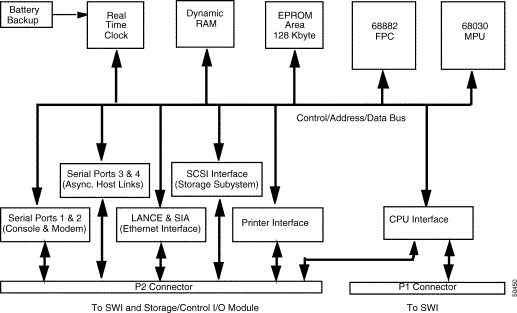
The VMEbus is designed for a multiprocessor application. A CPU card functions as bus master in a system controller with the capability of forcing read or write transfers to and from other cards on the VMEbus. To perform this function, the CPU must be in slot 1 of the upper 9-slot VME backplane. Bus arbitration is daisy-chained to the remaining slots in the backplane.
If the system is equipped with a redundant control subsystem, there are two system controllers. A CPU card is mounted in slot 1 of the redundant upper VME backplanes.
The on-board RAM (16 MB) is accessible by the 68030 MPU, Local Area Network Controller for Ethernet (LANCE), and VMEbus. Dynamic, RAS-only, RAM refresh is done every 8 ms by performing a memory cycle at each of the 512 row addresses. To accomplish this, once every 15 ms, the refresh timer requests that the RAM sequencer performs a column address strobe.
There are four 32-pin EPROM sockets on the CPU cards. Two different PROM memory banks (two PROMs per bank) are used, one for boot up and the other for the system application programs. During power up, the microprocessor reads two vectors from the PROM area: the initial stack pointer and the initial program counter.
The real-time clock provides seconds, minutes, hours, day, date, month, and year, in BCD 24-hour format. System administrators can reset the system clock through the Clock/Calendar Configuration screen from the System Configuration menu (refer to the Cisco VCO/4K System Administrator's Guide for more information). Automatic corrections are made for 28, 29 (leap year) and 30 day months. The internal backup battery for the clock has a typical life span of from three to five years.
This section contains a functional description of the major components of the CPU card.
Figure 2-9 shows the front panel layout of the CPU card. Two switches, RESET and ABORT, and four LED indicators (FAIL, STATUS, RUN and SCON) are located on the front panel of the card. The RESET switch forces a reset of all on-board devices and the VMEbus, but does not reset the system.
|
Note To reset the system, use the RESET button on the AAC. |
The CPU front panel also contains a connector for a remote reset switch and cable assembly that performs the same function as the RESET switch. Cisco Systems does not provide this switch and cable assembly and does not recommend its use.
The ABORT switch generates a Level 7 interrupt to the 68030 microprocessor. However, the VMEbus is not reset.
The red FAIL LED illuminates when the 68030 microprocessor stops processing due to a board failure condition. Users should compare this LED to the yellow STATUS LED to diagnose the failure condition. The STATUS LED indicates a halt condition on the microprocessor. A halt indication following a successful system reset indicates a software problem or a possible DRAM error. A halt on reset may indicate a firmware problem. The PROMs on the CPU card could be improperly installed (wrong location or not in socket), or the firmware may not be at the proper revision level.
|
Caution A FAIL condition indicates a severe problem that must be dealt with immediately to avoid prolonged loss of service. Reset the system controller from the AAC as a first course of action. If the FAIL condition continues, contact Cisco Systems Technical Support. |
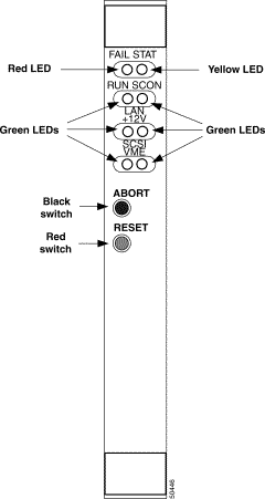
The green RUN and SCON LEDs remain illuminated during normal operation. The RUN LED shows that the 68030 microprocessor is executing a normal bus cycle. The SCON LED shows that the CPU is the system controller. A summary of front panel indicators is provided in Table 2-4.
| FAIL Red | STATUS Yellow | RUN Green | CPU STATUS |
|---|---|---|---|
Off | Off | Off | No power is applied to the CPU or the CPU is not the current local bus master. |
Off | Off | On | CPU is waiting for the cycle to complete. |
Off | On | Off | CPU is halted. |
Off | On | On | Normal operation. |
On | Off | Off | CPU is not the current local bus master and a board failure condition exists. |
On | Off | On | Board failure condition exists and the CPU is waiting for cycle to complete. |
On | On | Off | CPU is halted and a board failure condition exists. |
On | On | On | Complete board failure. |
The CPU card plugs into the Combined Controller Assembly through two standard DIN 41612 triple-row, 96-pin male connectors.
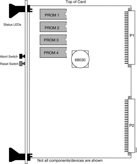
The CPU is a multipurpose OEM-supplied package modified by Cisco Systems for operation in a system. Modifications include the insertion of custom PROM chips in the firmware sockets. Figure 2-10 uses gray scaling to show PROM locations on the CPU card.
|
Caution Do not remove or reposition the jumpers on the CPU card. To do so may result in system failures and possible damage to the CPU card or to devices connected to it. Jumpers should remain in the factory-set position on the CPU card. |
The 128Kx8 PROM 1 contains firmware with the Low Kernel of the VRTX operating system.
The 128Kx8 PROM 2 contains firmware labeled High Kernel.
PROMs 3 and 4 contain standard EPROM for CPU operation.
The CPU card must be the first card plugged into the upper VME backplane of both the primary and redundant system controllers for proper VMEbus control.
|
Warning Read all instructions before attempting to remove or replace a card. To minimize the risk of injury from hazardous voltages, avoid contact with the backplane when removing or replacing system cards. Observe antistatic precautions when handling a card to avoid damaging sensitive CMOS devices. Wear a ground strap connected to the system equipment frame whenever removing or replacing cards or I/O modules. |
Control Circuit cards require slightly different procedures for removal and replacement. However, there are some common procedures to be followed before removing and after replacing a circuit card.
The CPU card contains the serial number required for the system's timeslot allocation license. This serial number was encoded in the card at the factory and cannot be altered. After the CPU card is replaced, the timeslot allocation license must be updated before the system will operate normally. For information on how to update the license, refer to the Cisco VCO/4K System Administrator's Guide.
A switch with one Combined Controller Assembly will be out of service until the failed Combined Controller Assembly is replaced. To remove and replace a Combined Controller Assembly in a nonredundant switch:
Step 2 Use a #1 Phillips-head screwdriver to remove the mounting screws/washers (five per bar) from the top and bottom PCB card retainer bars (see Figure 2-11) on the system. Keep the retainers and screws together in a safe place for replacement later.

Step 3 Remove and replace the failed Combined Controller Assembly(s).
Step 4 Power on the system, following the instructions in your Cisco VCO/4K System Maintenance Manual. The system should boot from hard disk; if it does not, press the Reset A button on the AAC. Normal operation should resume after the system has been fully initialized.
To remove and replace a CPU card in a switch with redundant control:
Step 2 Place the Combined Controller Assembly to be serviced in Standby mode; use the SELECT switch on the AAC to designate the other Combined Controller Assembly as Active.
Step 3 When the transition to standby is complete, remove the entire Combined Controller Assembly. Calls will be processed through the Active controller.
Step 4 When the service activity has been completed, restore power to the standby side.
Step 5 Press the RESET button of the serviced side on the AAC. The serviced Combined Controller Assembly should boot from hard disk. The update channel will be established and automatic file synchronization will be initiated.
Step 6 When file synchronization is completed, the serviced Combined Controller Assembly should be in standby mode. Return the Side SELECT on the AAC to auto, if desired.
To remove a CPU card:
Step 2 Remove the entire Combined Controller Assembly from active service (refer to the "Removing and Replacing System Controller Cards" section).
|
Caution Always remove the Combined Controller Assembly before removing the CPU card. Never remove a CPU card from a Combined Controller Assembly that is mounted in a system. |
Step 3 Use your thumbs to push the upper and lower ejectors away from the Combined Controller Assembly front panel. This action will pop the card from the SWI connectors.
|
Note Remove and replace cards using only enough force to disengage or engage the card from or into backplane connectors. Yanking cards from, or jamming cards into, the backplane can seriously damage connectors and result in operating problems which will be very difficult to isolate. |
Step 4 With both hands, grasp the Combined Controller Assembly on its top and bottom edges as you remove it from the card slot. Pull the Combined Controller Assembly from the card slot.
Step 5 Place the card on an antistatic mat or envelope.
Step 6 Use a 1/8-inch bladed screwdriver to loosen the captive mounting screws at the top and bottom of the CPU card. Do not remove the screws from the cards.
Step 7 Use your thumbs to push the upper and lower extractors away from the CPU card front panel. This action disconnects the card from the SWI connectors.
Step 8 Pull the CPU card away from the Combined Controller Assembly.
Step 9 Place the CPU card on an antistatic mat or an antistatic envelope.
|
Caution Always remove the Combined Controller Assembly before replacing the CPU card. Never replace a CPU card in a Combined Controller Assembly that is mounted in a system. |
To replace the CPU card:
|
Note Refer to your release notes and verify that the revision levels of the PROMs match the requirements of the generic software currently loaded in your VCO/4K system. |
Step 2 Grasp the replacement CPU card by the top handle and the bottom edge and align it with the top and bottom card guides of the Combined Controller Assembly.
Step 3 Push the CPU card in until it makes contact with the SWI connectors. Use your thumbs to push the extractors toward the front panel.
Step 4 Replace the screw at the top of the CPU card front panel.
Step 5 With both hands, grasp the Combined Controller Assembly on its top and bottom edges and align it with the top and bottom card guides of the card slot.
Step 6 Push the Combined Controller Assembly inward until it makes initial contact with the backplane.
Make sure the ejector levers are perpendicular to the front panel. Continue pushing the Combined Controller Assembly inward until it makes firm contact with the backplane. The hooks on the ejectors must be behind the front rail of the card slot. Use your thumbs to push the ejectors inward toward the front panel. The card should be fully seated into the backplane connectors when the levers are flush against the front panel.
Step 7 Grasp the replacement CPU card by the top handle and the bottom edge and align it with the top and bottom card guides of the Combined Controller Assembly.
Step 8 Push the card inward until it makes contact with the backplane.
Step 9 Firmly grasp the handles at the top and bottom of the CPU card and push the card toward the backplane. The card fits tightly into the backplane connectors and some force is required to seat the card back firmly into the backplane connectors.
Step 10 Use a 1/8-inch bladed screwdriver to tighten the mounting screws at the top and bottom of the CPU card.
Step 11 Refer to the "Removing and Replacing System Controller Cards" section and place the Combined Controller Assembly back in service.
Step 12 Reinstall the top and bottom PCB card retainer bars (see Figure 2-11). Use a #1 Phillips-head screwdriver to replace the mounting screws/washers (five per bar).
|
Caution The PCB card retainer bars must be installed for the system to meet NEBS Zone 4 Earthquake compliance. |
The Cisco VCO/4K System Maintenance Manual describes corrective maintenance procedures for host communications links. In addition to this manual, you should refer to the Cisco VCO/4K Standard Programming Reference or Cisco VCO/4K Extended Programming Reference for details relating to command and report formats. Cisco VCO/4K System Messages describes the network messages associated with problems detected with the host communications links.
If you are using the optional Ethernet Communications Package, refer to the Cisco VCO/4K Ethernet Guide for maintenance procedures.
Other reference materials include the OEM manuals supplied with the host computer I/O package and the modems used for the link (optional), and any documentation related to the communication and application packages to be run on the host computer.
To isolate and correct CPU card problems, perform the following steps.
|
Caution Initiating a reset on the CPU card in an Active Combined Controller Assembly will result in disruption of system service. Set the Combined Controller Assembly to Standby (redundant control) or be sure that such an interruption is acceptable prior to performing any of the following troubleshooting procedures. |
Step 2 Perform a reset by pressing and releasing the RESET switch on the AAC front panel. The LED on the hard disk drive should go ON and OFF intermittently. When the reboot is completed, the RUN, +12V, and SCON indicators should be illuminated.
Step 3 If the Combined Controller Assembly will not reboot, remove and reseat the CPU card into the Combined Controller Assembly. Perform a reset and observe the hard disk drive.
Step 4 Refer to the Cisco VCO/4K System Maintenance Manual for additional information on system level troubleshooting techniques. If all else fails, call Cisco Systems Technical Support.
The Combined Controller Assembly (CCA) consists of the following components:
The CPU is a high-performance, single-board computer that serves as the heart of the system controller.
The SWI provides an interface between the system controller and the following subsystems: Network Bus Controller 3 (NBC3), Alarm Arbiter Card (AAC), and redundant system controller.
The floppy disk drive is a 1.44-MB high-density, 3-1/2 inch, half-height floppy disk drive. The floppy disk drive is used to load software and make backup copies of the system database. You can also choose to store the system database, and log and trace files on floppy disk.
The SWI and floppy disk drive assembly also acts as a carrier for the CPU card.
Figure 2-12 shows the front of a VCO/4K and the location of the Combined Controller Assembly.
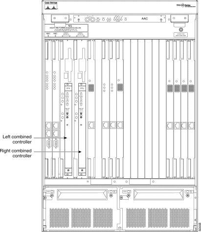
Figure 2-13 is a top view of the Combined Controller Assembly, showing its components.

Power Requirements: | +5 VDC |
|
| -48 VDC |
|
| -15 VDC |
|
Physical Dimensions: | Height: | 15.6 in. (396 mm) |
| Depth: | 12.1 in. (307 mm) |
| Width: | 0.79 in. (20 mm) |
The CPU performs the following system functions:
The CPU card incorporates a 68030 type 32-bit microprocessor, 16 MB of dynamic RAM, and 512 KB of ROM. A clock with battery backup supports time-stamped applications.
Microprocessor: | MC68030 (33 MHz) | |
Real Time Clock: | Programmable real-time clock with battery backup | |
Memory: | 16 MB of DRAM | |
Firmware: | 512 KB of EPROM | |
Physical Dimensions: | Height: | 9.2 in. (234 mm) |
| Depth: | 6.3 in. (160 mm) |
| Width: | 0.8 in. (19.8 mm) |
The 68030 microprocessor supports memory addressing and refreshing, and multiple I/O ports. The real-time clock is set through a system administration menu (refer to the Cisco VCO/4K System Administrator's Guide for more information). Figure 2-14 is a simplified block diagram of the CPU card.
The 68030 microprocessor operates at 33 MHz and includes an asynchronous 32-bit data bus and 32-bit address bus. Memory and I/O devices communicate with the CPU card over its local system bus.

The on-board RAM (16 MB) is accessible by the 68030 MPU and Local Area Network Controller for Ethernet (LANCE). The CPU refreshes dynamic, RAS-only, and RAM every 8 ms by cycling through the memory at each of the 512 row addresses. To accomplish this, once every 15 ms, the refresh timer requests that the RAM sequencer performs a column address strobe.
There are four 32-pin EPROM sockets on the CPU card. Two different EPROM memory banks (2 PROMs per bank) are used—one for bootup and the other for the system application programs. During powerup, the microprocessor reads two vectors from the EPROM area: the initial stack pointer and the initial program counter.
The real-time clock provides seconds, minutes, hours, day, date, month, and year in BCD 24-hour format. The Clock/Calendar Configuration screen from the System Configuration menu allows users to reset the system clock via system administration (refer to the Cisco VCO/4K System Administrator's Guide for more information). Automatic corrections are made for 28, 29 (leap year) and 30-day months. The internal backup battery for the clock has a typical life span of three to five years.
Two switches, RESET and ABORT, and four LED indicators (FAIL, STATUS, RUN, and SCON) are located on the front panel of the CPU card. The RESET switch forces a reset of all on-board devices, but does not reset the system.
|
Note To reset the system, use the RESET buttons on the AAC. |
The Combined Controller front panel also contains a connector for a remote reset switch and cable assembly that performs the same function as the RESET switch. Cisco Systems does not provide this switch and cable assembly and does not recommend its use.
The ABORT switch generates a Level 7 interrupt to the 68030 microprocessor.
The red FAIL LED illuminates when the 68030 microprocessor stops processing due to a board failure condition. Users should compare this LED to the yellow STATUS LED to diagnose the failure condition. The STATUS LED indicates a halt condition on the microprocessor. A halt indication following a successful system reset indicates a software problem or a possible DRAM error. A halt on reset may indicate a firmware problem. The PROMs on the CPU card could be improperly installed (wrong location or not in socket), or the firmware may not be at proper revision level.
|
Caution A FAIL condition indicates a severe problem that must be dealt with immediately to avoid prolonged loss of service. Reset the system controller from the AAC as a first course of action. If the FAIL condition remains, contact Cisco Systems Technical Support. |
The green RUN and SCON LEDs remain illuminated during normal operation. The RUN LED indicates the 68030 microprocessor is executing a normal bus cycle. The SCON LED indicates the CPU is the system controller. Table 2-5 describes the front panel status LEDs.
| FAIL Red | STATUS Yellow | RUN Green | CPU STATUS |
|---|---|---|---|
Off | Off | Off | No power is applied to the CPU or the CPU is not the current local bus master. |
Off | Off | On | CPU is waiting for cycle to complete. |
Off | On | Off | CPU is halted. |
Off | On | On | Normal operation. |
On | Off | Off | CPU is not the current local bus master and a board failure condition exists. |
On | Off | On | Board failure condition exists and the CPU is waiting for cycle to complete. |
On | On | Off | CPU is halted and a board failure condition exists. |
On | On | On | Complete board failure. |
The CPU card plugs into the SWI and floppy disk drive assembly through two standard DIN 41612 triple-row, 96-pin male connectors.
The CPU is a multipurpose, OEM-supplied package modified by Cisco Systems for operation in a system. Modifications include the insertion of custom EPROM chips in the firmware sockets.
|
Caution Do not remove or reposition the jumpers on the CPU card, as this may result in system failures and possible damage to the CPU card or to devices connected to it. Jumpers should remain in the factory-set position on the CPU card and should not be removed or changed. |
The 128Kx8 EPROM1 contains firmware with the Low Kernel of the VRTX operating system.
The 128Kx8 EPROM2 contains firmware labeled High Kernel.
EPROMs 3 and 4 contain boot EPROM for CPU operation.
DMA Controller: | 68450 (4 MHz) | |
Memory: | 64 KB Static RAM | |
Formatted Capacity: | 1.44 MB | |
Signal Interface: | SCSI |
|
Recording Method: | MFM |
|
Media Requirement: | 3.5-inch, high-density (2HD) floppy disks | |
Rotational Speed: | 300 rpm |
|
Read/Write Heads: | 2 heads |
|
Track Density: | 135 tracks per inch (tpi) | |
Data Transfer Rate: | 500 kbps |
|
Physical Dimensions: | Height: | 15.6 in. (396 mm) |
| Depth: | 12.1 in. (307 mm) |
| Width: | 1.58 in. (40 mm) |
The SWI is located on the Combined Controller Assembly along with the floppy disk drive and outer backplane. The SWI card generates the specific voltages that are used by the CPU card and the floppy disk drive and Storage/Control I/O Module. It also passes SCSI information to the floppy disk drive and the hard disk drive. The hard disk drive is located on the Storage/Control I/O Module.
The SWI provides a memory-addressable interface from the CPU to the NBC3 and the AAC. The SWI also passes power to the AAC (see Figure 2-15).
The NBC3 interface includes a 16-bit bidirectional data path and handshaking signals. This path carries command data and call setup data loaded into SWI registers by the system controller CPU. Two unidirectional 8-bit data channels allow communication between the A-side and B-side SWI cards in redundant systems.
All data transfers between the NBC3 and SWI, or between two SWIs, are performed by a 68450 four-channel bidirectional DMA controller. The DMA controller only transfers data to and from the SWI's on-board 64 KB of static RAM. The SWI cannot write data to and from the CPU as a bus master.
The 68450 is a four-channel DMA controller. Channels 0 and 1 are configured for 16-bit data transfers to and from the NBC3. Channels 2 and 3 are configured for 8-bit data transfers to and from the SWI in a redundant system configuration. Channels 0 and 2 are dedicated to incoming data; channels 1 and 3 are used for outgoing (relative to the SWI) data.
Logic on the SWI causes a DMA operation to terminate normally when the last byte/word of data is sent or received. When a data transfer is complete, the DMA controller interrupts the CPU. On the CPU's interrupt acknowledge cycle, the DMA controller returns the appropriate channel's normal interrupt vector.
If a bus error occurs while the DMA controller is in control of the internal SWI bus, the DMA controller terminates the bus cycle, aborts the transfer, sets the channel error register to indicate that a bus error occurred, and interrupts the CPU. On the CPU's interrupt acknowledge cycle, the DMA controller returns the appropriate channel's error interrupt vector.
Two sets of bidirectional registers are provided on the SWI. These registers are loaded by the CPU to send path setup information to the NBC3. Verify path setup information by reading the contents of these registers.
Static RAM on the SWI is isolated from the CPU so that DMA transfers to and from memory can occur without interrupting activity on the CPU. When CPU access to any on-board SWI device occurs, the current DMA cycle, if any, is completed before the CPU access takes place.
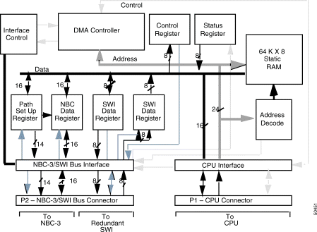
The signals between SWIs are carried on the control midplane. The signals to the AAC are carried to the control midplane and then through a ribbon cable to the AIC. The AAC then seats directly into the AIC. The connection between the SWI and the NBC3 is made through the control midplane.
The floppy disk drive is a 1.44-MB high-density, 3-1/2-inch, half-height floppy disk drive. Use the floppy disk to load software and make backup copies of the system database. Disk utilities are accessible from the Maintenance menu during system operation and from the Software Installation Utility diskette when this diskette is used to initialize the system.You can also choose to store the system database, and log and trace files on floppy disk. Refer to the Cisco VCO/4K System Administrator's Guide for more information.
The drive reads/writes to 3-1/2-inch double-sided, high density (2HD) floppy disks. Files are stored on the floppy drive in MS-DOS format. The floppy drive has a black ABS plastic front with a disk ejection button and a drive access LED indicator.
The front panel of the Combined Controller Assembly contains five LEDs.
Three SWI status LEDs are located at the top of the front panel. These LEDs are OFF when the card is operating normally. The red (top) LED is illuminated when either the system controller or the NBC3 fails. All LEDs are illuminated during system initialization.
The red 12VF LED located near the bottom of the panel shows a local 12-volt combined controller power failure.
The red HDD LED located below the 12VF LED shows hard disk drive activity.
System controllers require slightly different procedures for removing and replacing the other cards. Depending on whether you have a redundant or a nonredundant system, there are some common procedures to follow before removing and after replacing the combined controllers. These procedures are discussed in the following sections.
|
Caution Observe antistatic precautions whenever handling the Combined Controller Assembly to avoid damage to sensitive CMOS devices. Wear a ground strap connected to the system equipment frame whenever removing or replacing control circuit cards. |
A system with one Combined Controller (nonredundant systems) remains out of service until a failed Combined Controller Assembly is replaced.
To remove and replace a Combined Controller in a nonredundant system:
Step 2 Remove and replace the Combined Controller Assembly.
Step 3 Power on the system, according the instructions in the Cisco VCO/4K System Maintenance Manual. The system should boot from the hard disk. If it does not, press the RESET A button on the AAC. Normal operation should resume after the system is fully initialized.
To remove and replace a Combined Controller Assembly in a redundant system:
Step 2 Remove and replace the STANDBY Combined Controller Assembly. Calls will continue to be processed through the ACTIVE system.
Step 3 When the service activity is complete, use the system administration menus to place the STANDBY Combined Controller Assembly in ACTIVE mode. Refer to the Cisco VCO/4K System Administrator's Guide for more information. The update channel is established and automatic file synchronization is initiated.
To remove a Combined Controller Assembly:
Step 2 Use a #1 Phillips-head screwdriver to remove the mounting screws/washers (five per bar) from the top and bottom PCB card retainer bars (see Figure 2-16) on the system. Keep the retainers and screws together in a safe place for replacement later.
Step 3 Use your thumbs to push the upper and lower extractors away from the card front panel. This action disconnects the assembly from the backplane connectors.
Step 4 Pull the Combined Controller Assembly away from the card slot.
Step 5 Place the card on an antistatic mat or an antistatic envelope.
To replace a Combined Controller Assembly:
Step 2 Grasp the replacement Combined Controller Assembly by the top handle and the bottom edge and align it with the top and bottom card guides of the rack.
|
Warning Be sure to plug the Combined Controller Assembly into the slot marked for the Combined Controller Assembly. Plugging the Combined Controller into the wrong slot may cause serious damage to the controller. |
Step 3 Be sure the extractor levers are perpendicular to the front panel. Push the Combined Controller Assembly into the rack until it makes contact with the backplane. The hooks on the extractors must be behind the front rail of the rack.
Step 4 Reinstall the top and bottom PCB card retainer bars (see Figure 2-16). Use a #1 Phillips-head screwdriver to replace the mounting screws/washers (five per bar).
|
Caution The PCB card retainer bars must be installed for the system to meet NEBS Zone 4 Earthquake compliance. |
The CPU card contains the unique serial number required for the system's timeslot allocation license. This serial number was encoded in the card at the factory and cannot be altered. After the CPU card is replaced, you must update the timeslot allocation license before the system will operate normally. For information on how to update the license, refer to the Cisco VCO/4K System Administrator's Guide.
To remove a CPU card:
Step 2 Remove the Combined Controller Assembly. Refer to the "Removing a Combined Controller Assembly" section for more information.
|
Caution Always remove the Combined Controller Assembly before removing the CPU card. Never remove a CPU card from a Combined Controller Assembly that is mounted in a system. |
Step 3 Remove the screw at the top of the CPU card front panel.
Step 4 Use your thumbs to push the upper and lower extractors away from the CPU card front panel. This action disconnects the card from the SWI connectors.
Step 5 Pull the CPU card away from the Combined Controller Assembly.
Step 6 Place the CPU card on an antistatic mat or an antistatic envelope.
To replace the CPU card:
|
Caution Always remove the Combined Controller Assembly before replacing the CPU card. Never replace a CPU card in a Combined Controller Assembly that is mounted in a system. |
Step 2 Grasp the replacement CPU card by the top handle and the bottom edge and align it with the top and bottom card guides of the Combined Controller Assembly.
Step 3 Push the CPU card in until it makes contact with the SWI connectors. Use your thumbs to push the extractors toward the front panel.
Step 4 Replace the screw at the top of the CPU card front panel.
Step 5 Replace the Combined Controller Assembly. Refer to the "Replacing a Combined Controller Assembly" section section for more information.
Use the following steps to isolate and correct programs with the CPU card.
|
Caution Initiating a reset on the CPU card in an ACTIVE Combined Controller Assembly will result in disruption of system service. Set the Combined Controller to STANDBY (redundant control) or be sure that such an interruption is acceptable prior to performing any of the troubleshooting procedures described below. |
Step 2 Perform a reset by pressing and releasing the appropriate RESET switch on the AAC front panel. The hard disk drive access LED should go ON and OFF intermittently. When the reboot is complete, the RUN and SCON indicators should be illuminated.
Step 3 If the Combined Controller will not reboot, remove it and check that the CPU is properly seated. Perform a reset and observe the hard disk drive.
Step 4 If the Combined Controller resets but the login screen does not appear on the master console screen, the problem may be due to either the VDT or the connecting cable. Check the cable and refer to the OEM manual supplied with the VDT for troubleshooting procedures.
Step 5 Refer to the Cisco VCO/4K System Maintenance Manual for additional information on system-level troubleshooting techniques. If all else fails, call Cisco Systems Technical Support.
Refer to the Cisco VCO/4K System Maintenance Manual for additional information about system level troubleshooting techniques. If all else fails, call Cisco Systems Technical Support.
Problems with the floppy disk drive are shown in error messages generated when the operating system attempts to read or write files to the drive. These messages are displayed on the master console screen and stored in the system error log on the hard disk. A review of the error logs will reveal developing patterns of stored file errors. These errors may indicate impending failure of a floppy disk drive component. Messages associated with floppy disk drive errors begin with a "PRM" prefix. Cisco VCO/4K System Messages contains a complete listing of error messages with brief definitions.
Problems with the SWI are shown in error messages generated when the SWI/NBC3 interface fails. If such messages are discovered, refer to the Cisco VCO/4K System Administrator's Guide and the "Network Bus Controller 3 Card (NBC3)" section for additional troubleshooting information.
If error messages indicate stored file problems, look to the CPU card LEDs and verify these indicators. If the CPU card appears to be operating normally, use the Disk Utilities menu under the Maintenance menu to call up a directory of the drive (refer to the Cisco VCO/4K System Administrator's Guide). Observe the access LEDs on the floppy disk drive and hard disk drive. These LEDs should be illuminated as the operating system reads the directory.
The red SWI LED located at the top of the panel indicates a major alarm condition when either the system controller or the NBC3 fails.
The red 12VF LED located at the bottom of the panel indicates a local 12V combined controller power failure.
The red HDD LED located above the 12VF LED indicates hard disk drive activity.
The floppy disk drive access LED is illuminated when the drive is accessed for a read/write operation. This LED should illuminate under the following conditions:
The Network Bus Controller 3 (NBC3) is a special control circuit card that drives the communications bus (comm bus) and timeslot address bus, and generates the system clocks. The NBC3 also provides the data communication path between other control circuit cards and the rest of the system.
The intelligence of the NBC3 comes from an on-board 68360 microprocessor. The 68360 microprocessor memory includes 1 MB of RAM (selectable) and 256 KB of EPROM.
The 68360 microprocessor allows the NBC3 to serve as the comm bus master. The Switch Interface (SWI) functions as a direct memory access (DMA) interface to the NBC3 for communication with the other control circuit cards. Redundant NBC3 cards operate in active or standby mode, depending on which controller is selected as master through the Alarm Arbiter Card (AAC).
|
Caution Do not pull the active side NBC3 on an operating production switch. Pulling an active NBC3 can generate errors and impact traffic. If you suspect a problem with an NBC3 card and you wish to remove it, first switch sides to make it the standby side. |
The NBC3 uses dynamic random access memory (DRAM) for program storage. The program/application is downloaded from the CPU card to the NBC3 through the SWI.
The NBC3 implements special Phase Locked Loop (PLL) circuitry that allows for system synchronization to the network via incoming T1/E1 facilities, or to the central office (CO) composite clock from a Building Integrated Timing Source (BITS) signal, or to the internal clock.
The card is equipped with a Stratum 4 clock.
The NBC3 has connections for a DTG-2 mezzanine card. The DTG-2 mezzanine card functions the same as the full-size DTG card. You can use either DTG card in your system. However, the DTG-2 mezzanine card does not require its own card slot.
Microprocessor | MCG8EN360-25 |
Memory | 1, 2, 4, or 8 MB DRAM SIMM |
Power Requirements (Typical) | 5 Volts - 4000 mA |
System Synchronization: Clock Input Internal Reference Clock |
1.544 MHz ±75 Hz (bus) 1.544 MHz ± 40 Hz (standard) |
Physical Dimensions | Height: 15.6 in. (396 mm) |
Figure 2-17 is a block diagram of the NBC3 card.

As the master of the comm bus, the NBC3 performs the following communication functions:
The comm bus is a one-byte-wide half-duplex interface. This interface facilitates the transfer of messages between the port cards and the NBC3.
The NBC3 includes PLL circuitry that lets you synchronize system clocks from an internal or external source. Internally, the NBC3 generates the timeslot reference quadrature (Stratum 4) clock.
Externally, the NBC3 synchronizes the system with a 64-KHz BITS clock input or with any incoming T1 (1.544-MHz clock) stream or E1 (2.048-MHz clock) stream. It can synchronize to an internal 1.544- MHz Stratum 4 clock.
Table 2-6 describes the timing synchronization options on the NBC3.
.
| Timing Source | Description |
|---|---|
A central office 64 KHz bipolar BITS clock. | Signal comes from the BITS. The BITS signal supplies DS1 and/or composite clock timing reference to all the other clocks in the central office. Synchronizes the system to the network. Input is through a DB-9 connector on the NBC3 card front panel. 1 |
A 1.544 MHz internal clock reference that synchronizes the pulse code modulation (PCM) bus on T1/E1 data streams. This source does not synchronize the system to the network; it provides a clock source that is Stratum 4 compliant. This clock is normally used for short periods of time (a day or less) when the network timing signal is lost for standalone switch operation. | Stratum-4 Clock Oscillator on card has a 20-year accuracy rating of ±25 ppm (parts per million). Oscillator meets the requirements for Stratum 4.
|
An incoming T1, E1, or PRI facility that gets its timing from a network timing source. | Timing is sourced from an incoming T1 stream. Input is through a backplane connection. |
| 1A BITS clock cable kit is available that routes the BITS signals to the rear of the VCO/4K chassis. This allows easy access for external cabling. |
The BITS clock signals at the DB-9 (J8) connector on the face of the NBC3 card (and on the optional BITS clock rear conector) are listed in Table 2-7.
If the NBC3 is the last destination of the BITS clock signal, install a jumper at JP3 (Rev E0xR boards) or JP7 (Rev C0xR boards) to terminate the clock signal.
.
| Signal | Pin |
|---|---|
Bipolar, Twisted pair | 2 |
3 |
The NBC3 communicates with the control circuit cards through a 16-bit, DMA-controlled, bi-directional data bus between the NBC3 and the SWI card. The NBC3 translates information from control circuit cards into a serial or 8-bit parallel stream.
The interface is connected internally via one of the serial communications controllers within the CPU, which is controlled by the NBC3 application. The input channel transfers data from the control circuit cards to the NBC3. The output channel transfers data from the NBC3 to the control circuit cards.
Data is transferred to and from the NBC3 memory by the DMA controllers on the SWI that are directionally dedicated.
The NBC3 receives command messages from the control circuit cards through the two SWI DMA channels. Received messages are placed into one of the receive buffers on the NBC3. Individual messages are extracted from the receive buffer(s) and placed in the appropriate card output buffer. There is an output buffer for each card in the system.
The NBC3 sends messages to the control circuit cards through the SWI DMA channels. Messages are received from the cards during the card polling cycle, aggregated in one of NBC3 transmit buffers, and when the buffer is full, sends the messages to the control circuit cards.
The timeslot address information stream shares the path on the SWI to the NBC3 with the normal messaging. The NBC3 receives the information from the control circuit cards, after which the information is translated into serial or parallel data. The data is then sent to the cards equipped to receive and interpret translated information through either the high-speed serial interface or the comm bus on the backplane. Other cards receive path setup commands as part of the messages from the control circuit cards through the NBC3.
Table 2-8 lists the external interfaces for the NBC3 cards.
.
| Connections | VCO/4K |
|---|---|
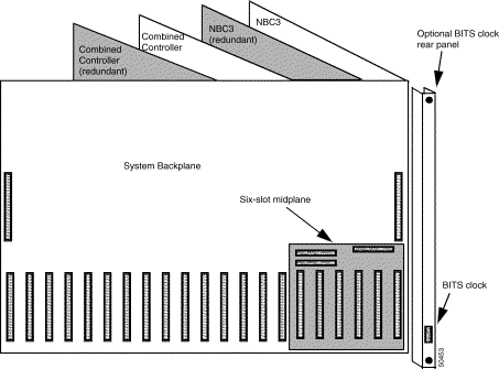
NBC3 to SWI | NBC3 and Combined Controller Assembly are connected to the six-slot midplane on the rear of the system backplane. |
BITS Clock | DB-9 connection on NBC3 card front panel.1 |
Debugging | EIA/TIA-232 connection on the NBC3 front panel. This is not for customer use. |
| 1A BITS clock cable kit is available that routes the BITS signals to the rear of the VCO/4K chassis. This allows easy access for external cabling. |
Figure 2-18 shows the NBC3 interconnections for VCO/4K systems.
.
The NBC3 card has seven status LEDs on the front panel, as shown in Figure 2-19. (The DTG-2 Presence LED is ON when a DTG-2 mezzanine card is installed on the NBC3 card.)
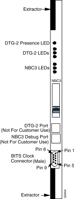
Table 2-9 lists the LED display for the DTG-2 mezzanine card.
| Card Status | Green | Yellow | Red |
|---|---|---|---|
Major DTG-2 card failure | Off | Off | On |
Minor DTG-2 card failure | Off | On | Off |
DTG-2 card is in standby, diagnostic, or out of service mode | On | Off | Off |
Table 2-10 lists the LED display for the NBC3 card.
| Card Status | Green | Yellow | Red |
|---|---|---|---|
Card plugged in (not initiated) | On | On | On |
Card initializing/self testing | On | Blinking | Off |
Card receiving download | Blinking | Off | Off |
OOS/Admin menu/standby/maintenance/diagnostics/remote | On | Off | Off |
Card operational/active | Off | Off | Off |
Major alarm (see Table 2-11 for details) | Off | Off | On |
Minor alarm (see Table 2-11 for details) | Off | On | Off |
Self test failure or stop processing/card failure or register dump | On | Off | On |
Table 2-11 lists the conditions that cause a major or minor alarm in the NBC3.
| Major Alarm | Minor Alarm |
|---|---|
Loss of synchronization timing | Unable to communicate due to NBC3 or control circuit cards failure |
Communications failure | Cannot obtain 32M lock |
Receive buffer overrun encountered | Cannot obtain 3M lock |
Transmit buffer overrun encountered | Receive buffer overrun pending |
Comm Bus failure | Transmit buffer overrun pending |
Table 2-12 lists the J1 pin assignments on the NBC3 card. J2 and J3 pin assignments are proprietary and, therefore, are not documented for customer use.
| Pin | Row A | Row B | Row C |
|---|---|---|---|
1 | DGND | Unused | DGND |
2 | DGND | Unused | DGND |
3 | DGND | Unused | DGND |
4 | DGND | Unused | DGND |
5 | Battery Return | Unused | Battery Return |
6 | Battery Return | Unused | Battery Return |
7 | Battery Return | Unused | Battery Return |
8 | Unused | Unused | Unused |
9 | Ring Voltage | Unused | Ring Voltage |
10 | Unused | Unused | Unused |
11 | Digital +5V | Unused | Digital +5V |
12 | Digital +5V | Unused | Digital +5V |
13 | Digital +5V | Unused | Digital +5V |
14 | +24 V | Unused | +24V |
15 | Battery (-48V) | Unused | Battery (-48V) |
16 | Battery (-48V) | Unused | Battery (-48V) |
17 | Battery (-48V) | Unused | Battery (-48V) |
18 | Analog (-15V) | Unused | Analog (-15V) |
19 | Analog (-15V) | Unused | Analog (-15V) |
20 | Analog (+15V) | Unused | Analog (+15V) |
21 | Analog (+15V) | Unused | Analog (+15V) |
22 | Card Address Bit 1 | Unused | Card Address Bit 0 |
23 | Card Address Bit 3 | Unused | Card Address Bit 2 |
24 | Card Address Bit 5 | Unused | Card Address Bit 4 |
25 | Card Address Bit 7 | Unused | Card Address Bit 6 |
26 | SRV | Unused | AB1 |
27 | DID | Unused | AB2 |
28 | RST | Unused | Serial Bus |
29 | CTV | Unused | CTT |
30 | GND | Unused | GND |
31 | GND | Unused | GND |
32 | DGND | Unused | DGND |
The NBC3 card is manufactured by Cisco Systems and includes firmware in the form of a PROM. All NBC3 jumpers except for the JP3 (Rev E) are factory set. If the NBC3 is the last destination of the composite clock signal, install a jumper at the J7/JP3 location to terminate the clock signal.
Figure 2-20 shows the location of the firmware PROM and the JP3 on the NBC3 Rev E card.
|
Caution Removing or repositioning the jumpers on an NBC3 card may cause system failures and damage to the card. Always verify that the jumpers are in their proper positions before installing or replacing an NBC3 card in the system. |
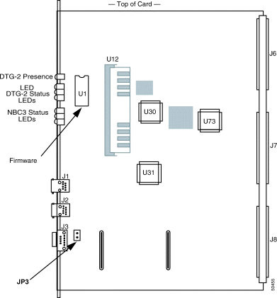
|
Note For Rev C cards the jumper is located at JP7, not JP3. |
The following card population rules apply to the NBC3:
This section describes how to remove and replace the NBC3 card. The NBC3 card can be removed and inserted while the system is powered on.
|
Caution Do not pull the active side NBC3 on an operating production switch. Pulling an active NBC3 can generate errors and impact traffic. If you suspect a problem with an NBC3 card and you wish to remove it, first switch sides to make it the standby side. |
|
Caution Observe antistatic precautions whenever handling the NBC3 to avoid damage to sensitive CMOS devices. Wear a ground strap connected to the system's equipment frame. |
Perform the following steps to remove an NBC3:
If the utility does not switch the system over, flip the SELECT toggle on the AAC to force the system to switch over. (Refer to the "Alarm Arbiter Card (AAC) with Alarm Interface Card (AIC)" section for more information.)
Step 2 If you have a redundant system and the NBC3 has a DTG-2 mezzanine card, verify that the DTG-2 is in standby mode and take the DTG-2 card out of service.
Step 3 If you have a nonredundant system, shut down the system. If you have a redundant system, shut down the standby side.
Step 4 Use a #1 Phillips-head screwdriver to remove the mounting screws/washers from the top and bottom PCB card retainer bars (see Figure 2-21) on the system. Keep the retainers and screws together in a safe place for replacement later.
Step 5 Disable the external alarm system to which the AAC might be connected.
Step 6 Disconnect all cables that are attached to the card (for example, BITS clock cable).
Step 7 Use your thumbs to pull the upper and lower extractors away from the card front panel. This action extracts the card from the backplane connectors.
Step 8 Pull the NBC3 free of the card slot.
Step 9 Place the card on an antistatic mat or envelope.
To replace an NBC3, perform the following steps:
Step 2 Refer to your release notes and verify that the revision levels of the PROMs match the requirements of the generic software currently loaded in the system.
Step 3 Verify that the switch and jumper settings on the replacement NBC3 are the same as those on the removed card.
Step 4 Grasp the replacement NBC3 by the top handle and the bottom edge and align it with the top and bottom card guides of the subrack.
Step 5 Make sure the extractor levers are perpendicular to the front panel. Push the NBC3 in until it makes contact with the master port subrack backplane. The hooks on the extractors must be behind the front rail of the subrack. Use your thumbs to push the extractors toward the front panel.
Step 6 If you are using the BITS clock option, reconnect the clock source to the DB-9 connector on the NBC3 front panel.
Step 7 Enable the external alarm system connected to the AAC terminals.
Step 8 If you have a nonredundant system, reboot the system. If you have a redundant system, reboot the standby side. (Refer to the Cisco VCO/4K System Maintenance Manual for more information.)
Step 9 If you have a redundant system, flip the SELECT toggle switch on the ACC to the AUTO position.
Step 10 The DTG-2 is automatically brought into service when the NBC3 is downloaded. If the DTG-2 card fails to automatically come into service, change the card status to active from the master console Card Maintenance menu. (Refer to the Cisco VCO/4K System Administrator's Guide for more information.)
Step 11 Reinstall the top and bottom PCB card retainer bars (see Figure 2-21). Use a #1 Phillips-head screwdriver to replace the mounting screws/washers (five per bar).
|
Caution The PCB card retainer bars must be installed for the system to meet NEBS Zone 4 Earthquake compliance. |
Because problems with the NBC3 critically affect system operation, the generic software provides numerous system error messages describing what type of NBC3 fault is detected. These error messages are fully described in Cisco VCO/4K System Messages.
A special set of messages which identify problems with T1 and NBC3 synchronization is also provided in Cisco VCO/4K System Messages.
When an NBC3 major alarm occurs in a nonredundant system, the AAC initiates a system reset. The CPU is cleared of all current data and all calls in progress are dropped. Service disruption lasts until the entire reset process is complete.
If the system reset fails to restore NBC3 operation on VCO/4K systems, replace the NBC3 card. See the "Replacing an NBC3" section for replacement procedures.
Verify that the system switched over so that the malfunctioning NBC3 is on the standby side. If the system did not switch over, flip the SELECT toggle on the AAC to force the system to switch over. (Refer to the "Alarm Arbiter Card (AAC) with Alarm Interface Card (AIC)" section for more information.)
If the reset fails to restore NBC3 operation, replace the NBC3 card. See the "Replacing an NBC3" section for replacement procedures.
![]()
![]()
![]()
![]()
![]()
![]()
![]()
![]()
Posted: Mon Aug 6 14:14:25 PDT 2001
All contents are Copyright © 1992--2001 Cisco Systems, Inc. All rights reserved.
Important Notices and Privacy Statement.