|
|

Appendix A lists the pinout signal summaries for Ethernet, Token Ring, asynchronous and synchronous serial interfaces, and for terminal and nonterminal devices. Also described are the pinouts for each applique type and each connector type.
Following is a list of the pinout signal summaries contained in this chapter:
The serial RS-232 lines on the communication server appear at the rear of the chassis as female telco 50-pin connectors. Each connector supports eight RS-232 lines. Each serial line card (CSC-16) has two such connectors.
Table A-1 describes the first two lines on a telco 50-pin connector. For each RS-232 signal, the color code is shown, as is the pin number on the telco 50-pin connector and the signal source. The remaining lines of the connector follow the same pattern. The signal names used in this chapter assume that the communication server is viewed as a DTE device.
| Line | Brief Name | Full Signal Name | Color Code | Pin Number | Signal Source |
|---|---|---|---|---|---|
| 1 | GND | Signal Ground | White-Blue | 26 | -- |
| 1 | TxD | Transmit Data | Blue-White | 01 | Server |
| 1 | RxD | Receive Data | White-Orange | 27 | Device |
| 1 | RING | Ring Indicate | Orange-White | 02 | Device |
| 1 | DTR | Data Terminal Ready | White-Green | 28 | Server |
| 1 | CTS | Clear to Send | Green-White | 03 | Device |
| 2 | GND | Signal Ground | White-Brown | 29 | -- |
| 2 | TxD | Transmit Data | Brown-White | 04 | Server |
| 2 | RxD | Receive Data | White-Slate | 30 | Device |
| 2 | RING | Ring Indicate | Slate-White | 05 | Device |
| 2 | DTR | Data Terminal Ready | Red-Blue | 31 | Server |
| 2 | CTS | Clear to Send | Blue-Red | 06 | Device |
In the simplest case of connecting a terminal (a DTE device) to the communication server, you need connect only Signal Ground, Transmit Data, and Receive Data signals. Table A-2 shows the pinouts.
| Signal | Name | Signal Source | Female DB-25 (DCE) |
|---|---|---|---|
| GND | Signal Ground | -- | Pin 7 |
| TxD | Transmit Data | Server | Pin 3 |
| RxD | Receive Data | Device | Pin 2 |
| RING | Ring Indicate | Device | -- |
| DTR | Data Terminal Ready | Server | -- |
| CTS | Clear to Send | Device | -- |
For more line control, connect the DTR output (pin 20) of the terminal to the CTS (Clear to Send) input line of the communication server (see Table A-3). Then configure the line with the modem cts-required subcommand of the line configuration command. In this mode, the communication server always asserts Data Terminal Ready (DTR) except when it briefly lowers the signal before entering the idle state. The communication server requires that the attached device assert the CTS input at all times. If CTS goes down, any connections are closed, and the communication server enters the idle state. The communication server will not respond to the activation character or form a reverse connection while the CTS signal is low on such a line.
| Signal | Name | Source | DB-25 (DCE) |
|---|---|---|---|
| GND | Signal Ground | -- | Pin 7 |
| TxD | Transmit Data | Server | Pin 3 |
| RxD | Receive Data | Device | Pin 2 |
| RING | Ring Indicate | Device | -- |
| DTR | Data Terminal Ready | Server | -- |
| CTS | Clear to Send | Device | Pin 20 |
If you want RTS/CTS or hardware flow control on a directly connected line, connect the Request To Send (RTS) output (pin 4) of the terminal to the CTS input of the communication server (see Table A-4). Then configure the line with the flowcontrol subcommand of the line configuration command. RTS/CTS flow control is not possible on a line using modem control.
| Signal | Name | Signal Source | Female DB-25 (DCE) |
|---|---|---|---|
| GND | Signal Ground | -- | Pin 7 |
| TxD | Transmit Data | Server | Pin 3 |
| RxD | Receive Data | Device | Pin 2 |
| RING | Ring Indicate | Device | -- |
| DTR | Data Terminal Ready | Server | -- |
| CTS | Clear to Send | Device | Pin 4 |
When you attach a DCE device with modem control to the communication server, you may want to use the pinout described in Table A-5.
| Signal | Name | Signal Source | Female DB-25 (DTE) |
|---|---|---|---|
| GND | Signal Ground | -- | Pin 7 |
| TxD | Transmit Data | Server | Pin 2 |
| RxD | Receive Data | Device | Pin 3 |
| RING | Ring Indicate | Device | Pin 22 |
| DTR | Data Terminal Ready | Server | Pin 20 |
| CTS | Clear to Send | Device | Pin 8 |
You may vary this construction. For example, if you set up the device so that CTS follows DCE, you will wire the communication server CTS input to pin 5 (standard CTS) instead of to pin 8 (standard DCE).
When you attach a dial-in modem (or a terminal switch with modem controls) to the communication server, configure the communication server line with the modem callin subcommand of the line configuration command.
The communication server handles the signals as follows:
If CTS does not go high within 20 seconds, the communication server drops its DTR output and returns to the idle state. If the CTS input is dropped at any time after the connection is completed, the communication server drops its DTR output and returns to the idle state.
If a device with modem control is to be attached to the communication server and accessed by telnet to that particular serial line on the communication server, then configure the line with the modem callout subcommand.
The communication server handles the signals as follows:
If the CTS input is not asserted within 20 seconds, the communication server drops its DTR output. The communication server advances to the next line in the rotary group if the first line is part of a rotary group. The communication server then raises DTR on that line and waits again for CTS.
If the communication server cannot complete a handshake with a line or runs to the end of a rotary group without successfully connecting, it closes the connection. If the CTS input drops at any time after the connection is completed, the communication server drops its DTR output, closes the connection, and returns to the idle state.
By default, the console ports on the CPU cards are wired for DCE. Both DSR and DCD are active when your system is running. The RTS signal tracks the state of the CTS input. The console port does not support flow control.Table A-6 shows the DCE wiring scheme for the console port.
| Pin | Signal | Description |
|---|---|---|
| 1 | Ground | Ground |
| 2 | RxD (in) | Receive Data |
| 3 | TxD (out) | Transmit Data |
| 4
5 | RTS
CTS | Ready To Send (pins 4 and 5 connected together)
Clear To Send |
| 6 | DSR (out) | Data Set Ready |
| 7 | Ground | Ground |
| 8 | DCD (out) | Data Carrier Detect |
An auxiliary port is supported for all processors. This is a DTE port on the CPU card
(CSC/3 and CSC/4) to which an RS-232 port from a CSU/DSU or protocol analyzer can be attached for access from the network.
The auxiliary port shares the ribbon cable between the processor card (CSC/3 or CSC/4) and the console port. The console-port end of the cable is split, so it has two RS-232 connectors at the connector-panel end: one for the console port and one for the auxiliary port. The processor-card end of the cable has one 50-pin ribbon connector, which connects to the console cable port on the processor card. Table A-7 shows the RS-232 signals used on this port.
| Pin | Signal |
|---|---|
| 2 | TxD (out) |
| 3 | RxD (in) |
| 7 | Signal Ground |
| 20 | DTR (out)1 |
| 24 | TxClk (out) |
As you use your product, it may become necessary to modify interfaces and build cables. This appendix provides the pinouts you will need to build these cables. If an applique contains jumpers that allow any modifications of the applique, that information also is included in the following sections.
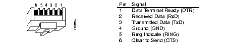
Figure A-1 shows an RJ-11 plug, and the pin assignments for an RJ-11 plug and socket.
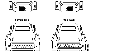
Both female (DTE) and male (DCE) adapters, which convert RJ-11 to DB-25, are shown in Figure A-2.
The pin signals and part numbers for the RJ-11 to DB-25 adapters are provided in
Table A-8.
| Part Numbers: | 74-0428 Female | 74-0427 Male | 74-0426 Female | 74-0425 Male | RJ-11 | |
|---|---|---|---|---|---|---|
| Signal | Direction | DCE | DCE | DTE | DTE | Jack |
| GND | -- | 7 | 7 | 7 | 7 | 4 |
| TxD | From chassis | 3 | 3 | 2 | 2 | 3 |
| RxD | To chassis | 2 | 2 | 3 | 3 | 2 |
| RING | To chassis | 22 | 22 | 5 | 5 | 5 |
| DTR | From chassis | 5 | 5 | 20 | 20 | 1 |
| CTS | To chassis | 20 | 20 | 5 | 5 | 6 |
The next three sections cover the pinouts for Ethernet and Token Ring appliques. The following appliques are included: 10BaseT pinout, Ethernet AUI pinout,Token Ring pinout.
The applique combines an RJ-45 connector for direct connection to an unshielded twisted-pair (UTP) network segment, a UTP tranceiver, and three green status indicators (see Figure A-3). The 10BaseT applique is compliant with IEEE 802.3.
The pinout for the RJ-45 connector is listed in Table A-9.
| Pin | Signal Name |
|---|---|
| 1 | TD+ |
| 2 | TD- |
| 3 | RD+ |
| 4 | Not used |
| 5 | Not used |
| 6 | RD- |
| 7 | Not used |
| 8 | Not used |
An attachment unit interface (AUI) transceiver must be used with most Ethernet products (the 10BaseT transceiver applique is an exception to this). Transceivers are available from a variety of sources for thick LAN, thin LAN, twisted-pair Ethernet, and other media.
Table A-10 lists the AUI pinout designations.
| Pin | Circuit | Description |
|---|---|---|
| 3 | DO-A | Data Out Circuit A |
| 10 | DO-B | Data Out Circuit B |
| 11 | DO-S | Data Out Circuit Shield (n/a) |
| 5 | DI-A | Data In Circuit A |
| 12 | DI-B | Data In Circuit B |
| 4 | DI-S | Data In Circuit Shield |
| 7 | CO-A | Control Out Circuit A (n/a) |
| 15 | CO-B | Control Out Circuit B (n/a) |
| 8 | CO-S | Control Out Circuit Shield (n/a) |
| 2 | CI-A | Control In Circuit A |
| 9 | CI-B | Control In Circuit B |
| 1 | CI-S | Control In Circuit Shield |
| 6 | VC | Voltage Common |
| 13 | VP | Voltage Plus |
| 14 | VS | Voltage Shield (n/a) |
| Shell | PG | Protective Ground |
There are several types of twisted-pair cable. Unshielded twisted-pair (UTP) cable should be 26 to 22 American wire gauge (AWG)--0.4 to 0.6 mm wire in a multiwire cable with 100-ohm impedance. The 802.3 specification states that the maximum length of a 10BaseT link segment is 100 meters or 328 feet of UTP wiring. Do not exceed these limits.
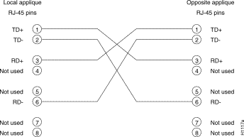
If you are not connected to a hub, and another 10BaseT transceiver applique is connected to the opposite end of your link, the UTP cabling must be crossed as shown in Figure A-4. The RD- and RD+ signals must be swapped with the TD- and TD+ signals. When the opposite end of your link is connected to a hub, the hub performs this crossover function, and it is not necessary to cross the cables.
The pinout for theToken Ring applique used with the CSC-1R and CSC-R16M cards is listed in Table A-11
| Pin | Signal |
|---|---|
| 1 | Receive0/R1- |
| 2 | Receive0/G6+ |
| 8 | Transmit0/B9+ |
| 9 | Ring Transmit0/O5- |
The following sections show the pinouts of the following appliques:
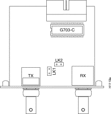
The G.703 network interface is the output port, consisting of two BNC connectors, adjacent to the approval symbol. The input port is connected by a ribbon cable to either a CSC-MCI or CSC-SCI interface card. Clock (timing) for the G.703 applique is derived from the network input at approximately 2048 Kbps (E1 speed). The G.703 supports only DTE. You must use two 75-ohm coaxial cables, of diameter 5mm, terminated in male BNC connectors, with maximum cable attenuation of 6 decibels dB at 1024 kHz. Attenuation characteristics should follow the root f law. The outer conductor is isolated from system earth. A total of six G.703 appliques can be mounted on a ladder plate, or a single applique can be mounted on an individual plate.
Figure A-5 shows the layout of the G.703 applique.
These warning notices apply to the Input Port, the port marked "SAFETY WARNING: see instructions for use."
Interconnection of the applique Input Port (the port marked "SAFETY WARNING: see instructions for use), directly, or by way of any other apparatus, with ports on other apparatus (marked or not so marked) may produce hazardous conditions on the network. Users should seek advice from a competent engineer before making such a connection.
The applique is approved as Independent of Host. As such, the applique is only approved for use with a host and with host attachments that are either type approved in their own right, or, if supplied after 1st March 1989, are covered by the terms of the General Approval number NS/G/1234/J/100003. A Host supplied under the terms of the General Approval number NS/G/1234/J/100003 satisfies the conditions of the paragraphs above.
The applique must not be modified in any way. Any form of modification invalidates the approval for connection and the warranty of the unit. The applique approval label must be visible externally. The approval label must not be detached from the applique, nor attached to the host.
The terms of the approval require that there must be a minimum distance (5 mm) between the applique and any other part of the host, including other appliques. This condition is met by default when the applique is installed in a chassis in accordance with the instructions. If voltages greater than 250 V are present in the host, users should refer to a competent safety engineer for advice.
It is a condition of the approval that a copy of these user instructions and safety warnings must be supplied with the host. Failure to provide the applique user instructions with the host will invalidate the applique approval.
Failure to install the applique in accordance with these instructions will invalidate the approval. If you experience difficulties, or are in any doubt, contact your service representative.
The X.21 applique, which is designed for domestic and international use, meets the CCITT specification for a DTE, VDE Class B, and FCC Class A, CSA C108.8. The applique can be set for either DTE or DCE mode, with default mode as DTE (shown in Figure A-6). Change the mode to DCE by changing the position of jumpers J1, J2, and J3 (as they are shown in Figure A-6). All three jumpers must be in the same position (DCE or DTE) in order for the applique to operate properly. Jumper J4 connects logic ground to chassis ground when in the default position, which is shown in Figure A-6.
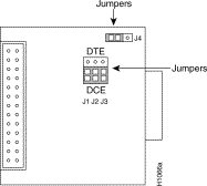
Table A-12 lists the pinout for the X.21 applique.
| Pin | Function | Direction |
|---|---|---|
| 1 | Shield Drain | -- |
| 2 | TXD - a | From chassis |
| 3 | Control - a | From chassis |
| 4 | RxD - a | To chassis |
| 5 | Indicate - a | To chassis |
| 6 | RxC - a | To chassis |
| 7 | DCE clock - a | From chassis |
| 8 | GROUND | -- |
| 9 | TXD - b | From chassis |
| 10 | Control - b | From chassis |
| 11 | RxD - b | To chassis |
| 12 | Indicate - b | To chassis |
| 13 | RxC - b | To chassis |
| 14 | DCE clock - b | From chassis |
| 15 | Not used | Not used |
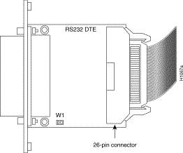
The RS-232 DTE applique has a male 25-pin D-type connector. The mode is fixed and printed on the applique (see Figure A-7). The internal ribbon cable attaches to the 26-pin connector shown in Figure A-7. Table A-13 lists the pinouts for the RS-232 DTE applique.
| Mnemonic | Pin | DTE Applique |
|---|---|---|
| RXD | 3 | To chassis |
| RXC(SCR) | 17 | To chassis |
| TXD | 2 | To DCE device |
| TXC(SCT) | 15 | To chassis |
| DTR | 20 | To DCE device |
| RTS | 4 | To DCE device |
| CTS | 5 | To chassis |
| CD | 8 | To chassis |
| LL | 9 | To DCE device |
| DSR | 6 | To chassis |
| TT(SCTE) | 24 | To DCE device |
| Chassis GND | 1 | -- |
| Signal GND | 7 | -- |
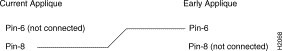
Very early MCI cards were shipped with an RS-232 DTE applique assembly designed by a third-party vendor. These older appliques, marked SCO-232, do not have any LEDs. If you are using this RS-232 DTE applique assembly on the other side of a link, the applique has Carrier Detect (CD) on pin 6 which is contrary to RS-232 specifications. When using this applique with an RS-232 DCE applique assembly, you must use a cable adapter or breakout box to change the cable as shown in Figure A-8. All other signals on the 25-pin cable should be straight through.
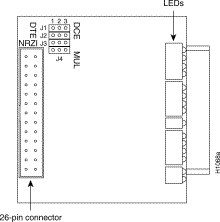
The RS-232 non-return to zero insertion (NRZI) applique has a female 25-pin D-type connector. An internal ribbon cable attaches to the 26-pin connector (see Figure A-9). Jumpers J1 and J2 set the mode (DCE or DTE), J3 sets the non-return to zero function, and J4 sets the downstream multidrop (MUL) option (in DCE or DTE) and half-duplex operation (HDX) in DCE mode. J4 also sets full-duplex (FDX) operation (see Table A-14).
| Jumper Pin Numbers | ||||
|---|---|---|---|---|
| Jumper | 1 | 2 | 3 | Function |
| J1 | Jumpered | Out | DTE1 | |
| J2 | Jumpered | Out | ||
| J1 | Out | Jumpered | DCE | |
| J2 | Out | Jumpered | ||
| J3 | Jumpered | Out | NRZI | |
| J3 | Out | Jumpered | NRZ | |
| J4 | Out | Jumpered | MUL2 | |
| J4 | Jumpered | Out | FDX3 | |
Table A-15 lists the pinout for the RS-232 NRZI applique.
| Signal Direction | |||
|---|---|---|---|
| Mnemonic | Pin | DTE Applique | DCE Applique |
| Shield | 1 | -- | -- |
| TxD | 2 | To DCE device | To chassis |
| RxD | 3 | To chassis | To DTE device |
| RTS | 4 | To DCE device | To chassis |
| CTS | 5 | To chassis | To DTE device |
| DSR | 6 | To chassis | To DTE device |
| Ground | 7 | -- | -- |
| DCD | 8 | To chassis | To DTE device |
| NC1 | 11 | Tied to ground for DTE | N/A |
| TxC | 15 | To chassis | To DTE device |
| RxC | 17 | To chassis | To DTE device |
| LL | 18 | To DCE device | To chassis |
| DTR | 20 | To DCE device | To chassis |
| SCTE | 24 | To DCE device | N/A |
| TM | 25 | N/A | To DTE device |
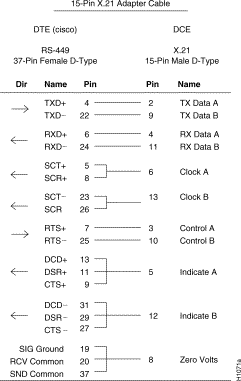
The RS-449 DTE applique contains a male 37-pin connector (the RS-449 DCE applique contains a female 37-pin connector). The mode is labeled on the circuit card (either RS-449 DTE or RS-449 DCE). The RS-449 DCE applique is shown in Figure A-10.
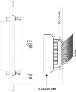
The RS-449 DCE applique requires that the clock be supplied from the MCI card or the SCI card. The DCE applique contains an additional jumper field (W2) which selects the transmit data clock source. Pins 1 and 1 of W2 are jumpered together causing the applique to expect to see the transmit clock on the serial clock transmit external (SCTE/TT) lines of the interface cable.
It is important that the DTE attached to this interface returns SCTE/TT along with its data to avoid cable-induced clock problems. This is the factory default, and it is the recommended setting for reliable operation at high data rates. If the DTE device does not return a clock on SCTE/TT, connecting pins 2 and 3 of W2 together causes the DCE applique to use the outgoing clock serial clock transmit (SCT/ST) instead of SCTE/TT.
The RS-449 DTE applique returns transmit clock on SCTE/TT. This is designed to compensate for clock phase shifting on long cables. It is important that the DCE device connected to the DCE applique modem be configured to accept SCTE/TT.
On both the DTE and DCE RS-449 appliques, pin 10 carries the local loopback (LL) signal. Use the software configuration subcommand loopback to invoke loopback to check out your installation or to verify that the applique is functioning correctly. When the loopback mode is invoked, the DCE applique responds to the LL signal by looping signals Send Data (SDA and SDB) to signals Receive Data (RDA and RDB), forming an outbound loopback and looping local data back to the MCI card.
Following is sample output of the loopback command for serial 0:
Router#configure terminal
Enter configuration commands, one per line.
Edit with DELETE, CRTL/W, and CRTL/U;end with CTRL/Z
interface serial 0
loopback
^z
Router#write memory
[ok]
Router#
The no loopback command returns the interface to normal function.
The RS-449 DTE applique is shown in Figure A-11.
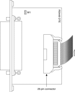
Table A-16 lists the pinouts of the RS-449 DCE and DTE appliques.
| Signal Direction | |||
|---|---|---|---|
| Mnemonic | Pin | DCE Applique | DTE Applique |
| Chassis ground | 1 | -- | -- |
| SDA (TXD+) | 4 | To chassis | To DCE device |
| SDB (TXD-) | 22 | To chassis | To DCE device |
| STA (SCT+) | 5 | To DTE device | To chassis |
| STB (SCT-) | 23 | To DTE device | To chassis |
| RDA (RXD+) | 6 | To DTE device | To chassis |
| RDB (RXD-) | 24 | To DTE device | To chassis |
| RSA (RTS+) | 7 | To chassis | To DCE device |
| RSB (RTS-) | 25 | To chassis | To DCE device |
| RTA (SCR+) | 8 | To DTE device | To chassis |
| RTB (SCR-) | 26 | To DTE device | To chassis |
| CSA (CTS+) | 9 | To DTE device | To chassis |
| CSB (CTS-) | 27 | To DTE device | To chassis |
| DMA (DSR+) | 11 | To DTE device | To chassis |
| DMB (DSR-) | 29 | To DTE device | To chassis |
| TRA (DTR+) | 12 | To chassis | To DCE device |
| TRB (DTR-) | 30 | To chassis | To DCE device |
| RRA (RLSD+,CD+) | 13 | To DTE device | To chassis |
| RRB (RLSD-,CD-) | 31 | To DTE device | To chassis |
| TTA (SCTE+) | 17 | To chassis | To DCE device |
| TTB (SCTE-) | 35 | To chassis | To DCE device |
| LL | 10 | To chassis | To DCE device |
| Signal Ground | 19, 20, 37 | -- | -- |
Figure A-12 provides the pinouts for constructing an X.21 to RS-449 transition cable. This is of particular importance for X.21 connections in the U.K. and Germany.
The HD V.35 applique carries the same signals as the old-style V.35 applique, but provides them on a smaller 26-pin D-type connector (the old-style applique used a 34-pin connector). The smaller 26-pin connector is male on all four versions of the HD V.35 cable, and the larger connector on each cable carries the male or female configuration.
Table A-17 provides pinouts for the HD V.35 applique (and cable) when used as a DTE or DCE interface.
| Applique | |||||
|---|---|---|---|---|---|
| DTE Pin | DCE Pin | Pin | Signal | Function | Direction |
| 26 | 26 | A | FG | Frame Ground | -- |
| 17 | 17 | B | SG | Signal Ground | -- |
| 23 | 24 | C | RTS | Request to Send | To modem |
| 24 | 23 | D | CTS | Clear to Send | To chassis |
| 22 | 25 | E | DSR | Data Set Ready | To chassis |
| 20 | 19 | F | RLSD | Receive Line Signal
Detect (Carrier Detect) |
To chassis |
| 19 | 20 | H | DTR | Data Terminal Ready | To modem |
| 21 | 22 | K | LT | Local Test (Loopback) | To modem |
| 2 | 4 | R | RD+ | Receive Data+ | To chassis |
| 12 | 14 | T | RD- | Receive Data- | To chassis |
| 6 | 5 | V | SCR+ | Serial Clock Receive+ | To chassis |
| 16 | 15 | X | SCR- | Serial Clock Receive- | To chassis |
| 4 | 2 | P | SD+ | Send Data+ | To modem |
| 14 | 12 | S | SD- | Send Data- | To modem |
| 5 | 6 | U | SCTE+ | Serial Clock Transmit External+ | To modem |
| 15 | 16 | W | SCTE- | Serial Clock Transmit External- | To modem |
| 1 | 3 | Y | SCT+ | Serial Clock Transmit+ | To chassis |
| 11 | 13 | a | SCT- | Serial Clock Transmit- | To chassis |
| 9 | -- | DCE/DTE | Selects DCE mode | -- | |
| 181 | -- | DCE/DTE | Selects DCE mode | -- | |
The HD V.35 applique options are listed by product number in Table A-18.
| Product Number | Mode | Plate Size | Chassis | Number of Interfaces |
|---|---|---|---|---|
| APP-IX1 | Dual | Individual | M, C | 1 HD V.35 |
| APP-JX1 | Dual | Individual | A+, A | 1 HD V.35 |
| APP-LX2 | Dual | Long | A+, A | 2 HD V.35 |
| APP-LX4 | Dual | Long | A+, A | 4 HD V.35 |
| APP-LX6 | Dual | Long | A+, A | 6 HD V.35 |
| APP-LX8 | Dual | Long | A+, A | 8 HD V.35 |
| APP-SX2 | Dual | Small | M, C | 2 HD V.35 |
| APP-SX4 | Dual | Small | M, C | 4 HD V.35 |
| APP-SX2E2 | Dual | Small | M, C | 2 HD V.35 and 2 Ethernet |
X = HD V.35
Table A-19 shows the four external interface cables available for the HD V.35 applique. The product numbers for these cables also are provided. The HD V.35 supports both DTE and DCE modes; the external V.35 cable attached to the applique determines this mode.
Table A-19 lists the HD V.35 external cable options by product number.
| Product Number | Mode1 | Cable Gender |
|---|---|---|
| CAB-VTM | DTE | Male-to-male |
| CAB-VTF | DTE | Male-to-female |
| CAB-VCM | DCE | Male-to-male |
| CAB-VCF | DCE | Male-to-female |
The HD V.35 applique is illustrated in Figure A-13.
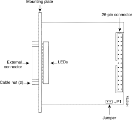
The HD V.35 applique has only one jumper (JP1), which selects SCT (from the chassis) or SCTE (to the chassis) as the timing source for SD when the applique is in DCE mode. The default is SCTE, selected when the jumper is in. To select SCT, remove the jumper.
|
|