|
|

This chapter discusses the maintenance of the ASM-CS and its components. Since your internetworking requirements may change over time, this chapter is designed to help you adapt as needed.
If any upgrades requiring card, firmware, or software replacement should be necessary, the appropriate documentation will be shipped with the replacement parts or upgrades you order. These replacement procedures are called configuration notes.
This chapter contains information on the following:
 | Caution Before performing any procedures in this chapter, review the following sections in Chapter 2: "Safety Recommendations," "Safety with Electricity," and"Preventing Electrostatic Discharge Damage." |
There are two ways to access the ASM-CS chassis interior: opening the chassis completely (including removing the top cover and front access panel) and opening only the front access cover and exposing the system card cage and installed cards. The following procedure includes both methods of chassis access.
The following tools are required for this procedure:
 | Warning Before accessing the chassis interior, turn off power to the chassis and unplug the power cord because high voltages may exist in or near the power supply. Use extreme caution when working near the power supply. Attach appropriate ESD protection before beginning the replacement procedure. |
Following is the procedure for accessing the chassis interior:
Step 1: Power the chassis down and unplug it from AC power.
Step 2: Disconnect all external cables from the chassis back panel. Note where these cables were connected, for reinstallation.
Step 3: If the chassis is rack mounted, remove it from the rack and transfer it to a desktop or work table.
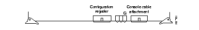
Step 4: Loosen the two thumb fasteners and remove the front access panel from the chassis (see Figure 5-1).
Step 5: Locate and remove the seven No. 1 Phillips screws securing the top of the chassis (see Figure 5-1). Set the top and screws aside.

Step 6: To reassemble the chassis, reverse steps 4 and 5.
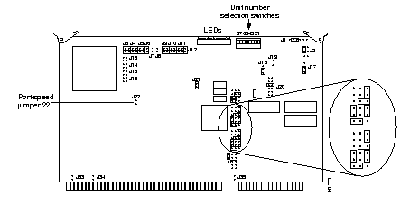
Some cards can be configured for different user-applications. For example, the CSC-MCI card has jumpers that allow you to change from data terminal equipment (DTE) mode to data communications equipment (DCE) mode depending upon your requirements. In addition, most cards have card numbering switches that allow you to reconfigure them for different slot positions in the ASM-CS.
An illustration of the card and a diagram and tables of the configurable jumpers and switches available on the card. Following is a listing of all the configurable cards in the ASM-CS.
Card numbers act as position markers for the system software and let the system know what cards are installed in what slots. The card numbers are assigned by way of a dual in-line package (DIP) switch located on the component side of the card. These switches are set so that each card has a unique card number. The only cards in the ASM-CS that will require unique card numbers are the asynchronous serial cards (CSC-16). Each card number should be unique within the set of CSC-16s installed in the ASM-CS.
Figure 5-2 shows a partial view of the component side of the processor card. The CSC/3 and CSC/4 processor cards contain the same components in the basic physical layout as illustrated.
For both processor cards, the 50-pin header in the center of the card is called the configuration register for the processor diagnostics. The following section "Configuration Register Settings," describes the settings for this register.
The processor cards have a 16-bit hardware configuration register: the far right 16 pairs of jumper pins on the 50-pin header in the center of the card (refer to Figure 5-3). Jumper bit (or position) 0 is the far right pair of pins. To set a bit to 1, insert a vertical jumper. To clear a bit to 0, remove the vertical jumper.
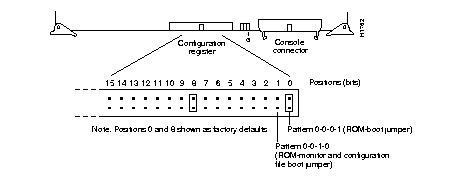
To change configuration register settings, turn off the system, set or clear the bits by inserting or removing jumpers, and restart the system, or change the jumper settings while the power is still on, and then give the privileged command reload. It is not necessary to remove the processor card from the backplane to change the jumper setting. Figure 5-3 shows the configuration register with the factory settings for CSC/3 and CSC/4.
The lowest four bits of the processor configuration register (bits 3, 2, 1, and 0) form the boot field (see Table 5-1). The boot field specifies a number in binary. If you set the boot field value to 0, you must boot the operating system manually by giving a b (or boot) command to the system bootstrap program. If you set the boot field value to 1 (the factory default), the system boots using the default ROM software. If you set the boot field to any other bit pattern, the system uses the resulting number to form a boot file name for netbooting. For example, a jumper configuration of 0-0-1-0 (bits 3-0) would be used when using the boot system flash feature with the Flash memory card.
| Action/File Name | Bit 3 | Bit 2 | Bit 1 | Bit 0 |
|---|---|---|---|---|
| bootstrap mode | 0 | 0 | 0 | 0 |
| ROM software | 0 | 0 | 0 | 1 |
| cisco2-csc4 | 0 | 0 | 1 | 0 |
| cisco3-csc4 | 0 | 0 | 1 | 1 |
| cisco4-csc4 | 0 | 1 | 0 | 0 |
| cisco5-csc4 | 0 | 1 | 0 | 1 |
| cisco6-csc4 | 0 | 1 | 1 | 0 |
| cisco7-csc4 | 0 | 1 | 1 | 1 |
| cisco10-csc4 | 1 | 0 | 0 | 0 |
| cisco11-csc4 | 1 | 0 | 0 | 1 |
| cisco12-csc4 | 1 | 0 | 1 | 0 |
| cisco13-csc4 | 1 | 0 | 1 | 1 |
| cisco14-csc4 | 1 | 1 | 0 | 0 |
| cisco15-csc4 | 1 | 1 | 0 | 1 |
| cisco16-csc4 | 1 | 1 | 1 | 0 |
| cisco17-csc4 | 1 | 1 | 1 | 1 |
Bit 8 in the configuration register controls the console Break key. Setting bit 8 to 1 (the factory default) causes the processor to ignore the console Break key. Clearing bit 8 to 0 causes the processor to interpret Break as a command to force the system into the bootstrap monitor, thereby suspending normal operation.
The system creates a boot file name as part of the automatic configuration processes. To form the boot file name, the system starts with cisco and links the octal equivalent of the boot field number, a dash, and the processor type name. Table 5-1 lists the default boot file names or actions for the CSC/4 processor. The list is the same for the CSC/3 processor card, with csc3 substituted for csc4.
Bit 9 in the configuration register controls the use of a secondary bootstrap procedure when netbooting. If inserted, a secondary bootstrap with the filename boot-csc4 (or csc3) is first loaded into the system over the network. This bootstrap image then loads in the desired boot file, completing the netbooting process.
Bit 10 in the configuration register controls the host portion of the Internet broadcast address. Setting bit 10 causes the processor to use all zeros; clearing bit 10 (the factory default) causes the processor to use all ones. Bit 10 interacts with bit 14, which controls the network and subnet portions of the broadcast address.
Table 5-2 lists the combined effect of bits 10 and 14.
| Bit 14 | Bit 10 | Address (<net><host>) |
|---|---|---|
| out | out | <ones><ones> |
| out | in | <zeros><zeros> |
| in | in | <net><zeros> |
| in | out | <net><ones> |
Bits 11 and 12 in the configuration register determine the baud rate of the console terminal. Table 5-3 lists the bit settings for the four available baud rates (the factory default is 9600).
| Baud | Bit 12 | Bit 11 |
|---|---|---|
| 9600 | 0 | 0 |
| 4800 | 0 | 1 |
| 1200 | 1 | 0 |
| 2400 | 1 | 1 |
Bit 13 in the configuration register determines the system response to a boot-load failure. Setting bit 13 causes the system to load operating software from ROM after five unsuccessful attempts to load a boot file from the network. Clearing bit 13 causes the system to continue attempting to load a boot file from the network indefinitely. By factory default, bit 13 is cleared to 0.
Bit 14 in the configuration register controls the network and subnet portions of the Internet broadcast address. Setting bit 14 causes the system to include the network and subnet portions of its address in the broadcast address. Clearing bit 14 causes the system to set the entire broadcast address to all ones or all zeros, depending on the setting of bit 10. By factory default, bit 14 is cleared to 0. See Table 5-2 for the combined effect of bits 10 and 14.
Bit 15 in the configuration register controls factory diagnostic mode in the system. Setting bit 15 causes the system to produce detailed CPU self-check messages, to automatically prompt for interface addresses (not look for addresses on the network), to not read configuration files or nonvolatile memory, and to automatically set to diagnostic tracing modes using the debug commands. Clearing bit 15 (the factory default) causes the system to operate normally.
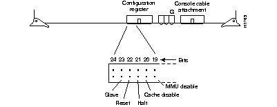
Bits 20 through 23 (the four pairs of pins on the far left of the 50-pin header) are not used in normal operation; however, they can be used to invoke the Slave mode, External Reset function, Halt Processor, and Cache Disable mode functions (respectively) on any processor card, and the MMU disable mode on the CSC/4 card (see Figure 5-4).
Figure 5-4 shows the optional jumper configurations. This is an edge-on view of the configuration register on a processor card installed in the backplane.
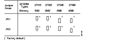
The CSC/3 and CSC/4 processor cards have configurable jumpers that control critical memory functions for the different sizes of electrically-erasable read-only memories (EPROMs) that can be installed. These EPROM jumpers are changed only when the EPROM memory sizes are changed. Do not change these from their default unless you are instructed to do so when the software is changed.
Figure 5-5 shows the positions of jumpers W51-W53 on the CSC/3, and Figure 5-6 shows the positions of jumpers W51-W52 on the CSC/4.
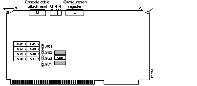
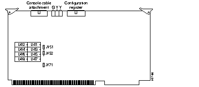
Figure 5-7 and Figure 5-8 show the EPROM jumper settings for the CSC/3 and CSC/4.

The following sections discuss the various configuration changes that can be made to the CSC-MCI card.
For the MCI card, card numbers are assigned by setting a dual in-line package (DIP) switch called the card numbering switch (S1), which is located toward the back of the card, near the bus edge connector (see Figure 5-9).
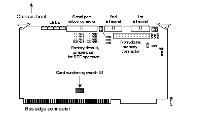
Table 5-4 shows the switch (S1) settings for assigning card number 0 to the MCI card.
| Card Number | S1-1 | S1-2 | S1-3 | S1-4 |
|---|---|---|---|---|
| 0 | Off | Off | Off | Off |
Jumpers at positions W51 and W41 control the serial ports 0 and 1 in DCE mode on the MCI card. In addition to jumper changes on the MCI card for DCE operation, you must configure the clock rate on the serial interface of the interface card using the clockrate speed interface subcommand (where speed is the bit rate of the interface in bits per second [bps]). The applique must be DCE (or configured as DCE) to generate the clock signals. Refer to the related Configuration and Reference publication for information on this subcommand.
Most DTE interfaces require a Normal External Transmit Clock (SCTE) signal. All DCE interfaces require a Internal Transmit Clock (SCT) noninverted signal.
The MCI card clocking options are controlled by jumper areas W40 through W53. The last two columns of this table (DTE and DCE) indicate the settings that should be used with either a DTE or DCE appliques. Unless specifically noted, all MCI cards are shipped with the factory default set to work with the DTE appliques. These appliques require external clocking; the CSU/DSU provides the clocking for the circuit.
Occasionally, delays occur between the SCTE clock and the transmit data that may push the data transition out to the point where using an inverted clock is appropriate (jumpers W42 and W52 for the MCI). Both ends of the wire may have variances that differ slightly. Typical delays indicate that the inverted clock may be appropriate above 1.3 MHz, depending upon the DTE-clock-to-data skews and setup required, and allowing some margin for temperature, cable, and other variables. Some DCE will not accept SCTE, so SCT must be used. Inverting the clock may be the only way to compensate for the cable length and circuit delays in the DTE and DCE.
Table 5-5 lists the jumper settings for the MCI clock options.
X = Recommended setting
x = Available, but not recommended
The CSC-MCI card provides up to two Ethernet ports (only one can be used with the ASM-CS). The CSC-MCI card provides grounding options to accommodate the differences between the Ethernet Version 1 and IEEE 802.3 electrical specifications. Ethernet Version 1 permits certain signals to float, whereas IEEE 802.3 requires the signals to be grounded. Inserting a jumper grounds a signal, and removing a jumper allows the signal to float. The factory default is to ground all signal pairs, which is compatible with both Ethernet and IEEE 802.3 requirements.
Table 5-6 lists the grounding options for the CSC-MCI card.
| Jumper Pair | Signal Description | Interface |
|---|---|---|
| W90 | Receive Pair Shield | First Ethernet |
| W91 | Transmit Pair Shield | First Ethernet |
| W92 | Power Pair Shield | First Ethernet |
| W60 | Power Pair Shield | Second Ethernet |
| W61 | Transmit Pair Shield | Second Ethernet |
| W62 | Receive Pair Shield | Second Ethernet |
Jumpers W94 and W93 are 3-pin jumpers that select between Ethernet and IEEE 802.3 electrical levels. Jumper W94 controls the first Ethernet and jumper W93 controls the second Ethernet. The factory default is to select IEEE 802.3/Ethernet Version 2. This setting must be changed to operate with an Ethernet Version 1 transceiver. Using the card orientation shown in Figure 5-9, place a jumper on the lower pair of pins to select IEEE 802.3 or Ethernet Version 2, or on the upper pair of pins to select Ethernet Version 1.
Software-readable switches 1-3 on the front edge of the CSC-1R card (see Figure 5-10) control card numbering within the chassis (switches 4-8 have no function). Configure the switches on the CSC-1R card to select the desired card number.
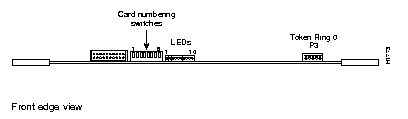
The card-numbering switches (1-3) are listed in Table 5-7 as they appear in Figure 5-10 from left to right.
| Card Number | Switch 1 | Switch 2 | Switch 3 |
|---|---|---|---|
| 0 | Down | Down | Down |
Down = switch is off
The following sections discuss the configuration requirements of the CSC-R16M card.
The speed of the CSC-R16M card is configurable. Jumper area J22 configures the CSC-R16 for either 4-Mbps or 16-Mbps operation (see Figure 5-11). No jumper at jumper area J22 (the factory default setting) selects 16-Mbps Token Ring operation, while installing a jumper at location J22 selects 4-Mbps Token Ring operation. The spare jumper to use at J22 is placed on the posts at jumper area J21. CSC-R16 cards are shipped configured to run at 16 Mbps (J22 has no jumper).
The card number of the CSC-R16M is selected through the use of software-readable dual in-line package (DIP) switches on the front edge of the card. Only switches 1-3 are used. Figure 5-12 shows these switches on the card front edge as viewed from left to right.
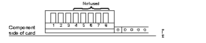
Table 5-8 lists the card numbering assigned to the CSC-R16M.
| Card Number | Switch 1 | Switch 2 | Switch 3 |
|---|---|---|---|
| 0 | Down | Down | Down |
Down = switch is off
The CSC-16 card, shown in Figure 5-13, is a 16-port asynchronous serial attachment; it is also called the communication server serial line card and is the primary card in the ASM-CS. The CSC-16 card LED indicators and rotary switch are discussed in Appendix B, "Reading LED Indicators."

The switch SW1 controls selection of the system bus memory unit number. SW1-2 should be on, and SW1-1 and SW1-3 through SW1-8 should be off.
Figure 5-14 shows the SW1 default switch settings for the CSC-16.

Table 5-9 lists the settings for SW1-9 through SW1-12, which are optional, and determine the unique card numbers up to the maximum number of seven CSC-16 cards. The default setting is card number 0.
| Card No. | 9 | 10 | 11 | 12 |
|---|---|---|---|---|
| 0 | Off | Off | Off | Off |
| 1 | Off | Off | Off | On |
| 2 | Off | Off | On | Off |
| 3 | Off | Off | On | On |
| 4 | Off | On | Off | Off |
| 5 | Off | On | Off | On |
| 6 | Off | On | On | Off |
The ASM-CS uses the model MAS-11 or MAS-11B power supplies. In the U.K., the ASM-CS uses the model MAS-26 power supply. If you have determined that you have a power supply problem, contact your nearest service representative.
Before making the call, verify the input voltage of your system by checking the label next to the power switch on the rear of the chassis and have the following information available:
The ASM-CS uses the model MAS-10 or MAS-10B blower vent assemblies for system cooling. If you determine that you have a cooling system problem, contact your nearest service representative.
Before making the call, verify the input voltage of your system by checking the label next to the power switch on the rear of the chassis and have the following information available:
|
|