|
|

Product Numbers: CSC/4=, CSC/4BU=, CSC/4BXU=, CSC/4BDU=, CSC/4XU=, CSC/4DU=, CSC/4SU=, CSC-4SP, CSC-4U, and all software maintenance release kits that operate with the CSC/4.
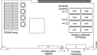
This document contains instructions for installing the CSC/4 processor card (shown in Figure 1) and for replacing erasable programmable read-only memory (EPROM) components to upgrade the system software. The card is used in routers with the standard system bus (the Multibus) or in AGS+ routers with a high-speed ciscoBus. Use the procedures in this document to install a new CSC/4 card and, if required later, to upgrade your software. The sections in this document cover the following:
The CSC/4 processor card contains a 25 megahertz (MHz) MC68EC040 microprocessor and 16 megabytes (MB) of random access memory (RAM), and supports up to 8 MB of read-only memory (ROM). The central processor contains the bootstrap program that initializes the system, and diagnostics that can be run on the system and its memory. The card contains a hardware configuration register, which can be configured to set up special system functions such as setting baud rates and specifying boot file names. The card also provides the connection for the system console port and for an optional auxiliary port to which you can connect external equipment (such as test equipment or another router). A partial component-side view of the card is shown in Figure 2.
The following sections discuss configuring the CSC/4 processor card (shown in Figure 1).
On the CSC/4 processor card, the 50-pin header in the center of the front edge of the card is used as a configuration register for processor functions and diagnostics. The following section describes the settings for this register. Figure 2 shows a partial component-side view of the processor card.
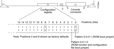
The processor card has a 16-bit hardware configuration register: the far right 16 pairs of jumper pins on the 50-pin header in the center of the card. (Refer to Figure 3.) Bit 0 (or position 0) is the far right vertical pair of pins. To set a bit to 1, insert a vertical jumper. To clear a bit to 0, remove the vertical jumper. Figure 3 shows the configuration register with the factory settings for the CSC/4.
To change configuration register settings, turn off the system, set or clear the bits by inserting or removing jumpers, and restart the system (or change the jumper settings while the power is still on, and then give the privileged command reload). It is not necessary to remove the processor card from the backplane or to turn off the power to change a jumper setting.
The lowest four bits of the processor configuration register (bits 3, 2, 1, and 0) form the boot field. The boot field specifies a number in binary. If you set the boot field value to 0, you must boot the operating system manually by giving a b (or boot) command to the system bootstrap program. If you set the boot field value to 1 (the factory default), the system boots using the default ROM software. If you set the boot field to any other bit pattern, the boot system commands override the default boot filenames when netbooting. For example, a jumper configuration of 0-0-1-0 (bits 3 through 0) is used when using the boot system flash command with the Flash memory card.
The system creates a boot filename as part of the automatic configuration processes. To form the boot filename, the system starts with cisco and links the octal equivalent of the boot field number, a dash, and the processor type name.
Table 1 lists the default boot filenames or actions for the CSC/4.
Table 1 Default Boot Filenames—Boot Field Jumpers
Note The four bits after the boot field (bits 4, 5,
6, and 7) in the configuration register are unused and must be left cleared (0).
Bit 8 in the configuration register controls the console Break key. Setting bit 8 to 1 (the factory default) causes the processor to ignore the console Break key. Clearing bit 8 to 0 causes the processor to interpret Break as a command to force the system into the bootstrap monitor, suspending normal operation.
Bit 9 in the configuration register controls the use of a secondary bootstrap procedure when netbooting. If this bit is set to 1, a secondary bootstrap (with the filename boot-csc4) is first loaded into the system over the network. This bootstrap image then loads in the desired boot file, completing the netbooting process.
Bit 10 in the configuration register controls the host portion of the Internet broadcast address. Setting bit 10 causes the processor to use all zeros; clearing bit 10 (the factory default) causes the processor to use all ones. Bit 10 interacts with bit 14, which controls the network and subnet portions of the broadcast address.
Table 2 shows the combined effect of bits 10 and 14. This effect is overridden by values set in NVRAM using the ip broadcast address command.
Table 2 Configuration Register Settings for Broadcast Address Destination
Bits 11 and 12 in the configuration register determine the baud rate of the console port. Table 3 shows the bit settings for the four available baud rates. (The factory default is 9600 baud.)
Table 3 System Console Port Baud Rate Settings
Bit 13 in the configuration register determines the system response to a boot-load failure. Setting
Bit 14 in the configuration register controls the network and subnet portions of the Internet broadcast address. Setting bit 14 causes the system to include the network and subnet portions of its address in the broadcast address. Clearing bit 14 causes the system to set the entire broadcast address to all ones or all zeros, depending on the setting of bit 10. By factory default, bit 14 is cleared to 0. See Table 2 for the combined effect of bits 10 and 14.
Bit 15 in the configuration register controls the factory diagnostic mode in the system. Setting bit 15 causes the system to produce detailed CPU self-check messages, to automatically prompt for interface addresses (not look for them on the network), to not read configuration files or NVRAM, and to automatically set to diagnostic tracing modes using the debug commands. Clearing bit 15 (the factory default) causes the system to operate normally. Bit 15 is also used for password recovery.
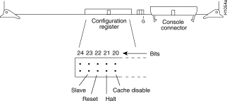
Bits 16 through 19 and bit 24 are not currently used.
Bits 20 through 23 (the four pairs of pins toward the far left of the 50-pin header) are not used in normal operation; however, they can be used to invoke the Slave mode, External Reset function, Halt Processor, and Cache Disable mode functions (respectively) on any processor card. Figure 4, which shows the optional jumper configurations, represents a partial front-edge view of the configuration register on a processor card installed in the card cage.
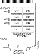
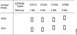
The CSC/4 processor card has configurable jumpers that control critical memory functions for the different sizes of erasable programmable read-only memories (EPROMs) that can be installed. These jumpers are changed only when the EPROM memory sizes are changed. Do not change these jumpers from their default settings unless you are instructed to do so when the software is changed. Figure 5 and Figure 6 show the positions of jumpers W51 and W52 on the CSC/4 card.
Before installing the CSC/4, ensure that your system meets the following prerequisites:
The CSC/4 processor card operates in modular router chassis (AGS+, A, M, or C) that are running System Software Release 9.0 or later, or in the ASM-CS (and MSM) modular communication server that is running System Software Release 9.1 or later. You can display the version of the software with the EXEC command show version. The current system software is displayed in the first line of the output, a sample of which follows:
If your system is running pre-9.0 software, contact a service representative for information on upgrades.
Verify that you received all of the following parts:
You need some or all of the following tools to perform the following procedures. Before you begin, read through the procedure to determine which tools you need for your chassis.
Electrostatic discharge (ESD) is a discharge of stored static electricity that can damage equipment and impair electrical circuitry. It occurs when electronic components are improperly handled and can result in complete or intermittent failures.
Following are guidelines for preventing ESD damage:
For safety, periodically check the resistance value of the antistatic strap. The measurement should be between 1 and 10 mega ohms.
If you are upgrading from a CSC/1 or a CSC/2 to a CSC/4 processor card, follow this procedure before installing the new CSC/4 card. If not, proceed to the section "Installation," on page 10.
Because the CSC/4 card is faster than the CSC/1 and CSC/2 cards, a system upgrade will cause spurious bus errors. To avoid these errors, copy the configuration file to a host on your network before removing the older processor card.
Follow these steps to copy your configuration file to a remote host. You will retrieve the file after the new CSC/4 is installed. The following procedure includes the steps for creating a temporary file; skip step 1 if you already have a usable file.
Step 2 Return to the router enable mode. Step 3 Upload the configuration to the temporary file using the privileged command write network. Step 4 The system will prompt you for a host name or address and the file name. Enter the address and name of the file you just created, or select a host that can act as a TFTP server. Sample output of the previous steps follows:
The !!!! and [ok] indicate that the operation was successful and that the configuration is safely stored in the temporary file on the TFTP file server. A failure is indicated with ... [timed out] or [failed]. A failure indicates a net fault or the lack of a writable, readable file on the TFTP server.
When the CSC/4 is installed correctly, retrieve the configuration file you stored as follows:
Step 2 Use the command write term to verify that the configuration is present in the running memory of the router. The configuration will be written to the terminal screen. Step 3 Save the configuration into the nonvolatile memory with the command write memory.
The following sections describe the procedures for installing the CSC/4 card in your chassis. The CSC/4 operates in any Cisco Systems modular chassis: A-type, M, or C. You will install the CSC/4 card in the system card cage of the chassis. Before proceeding, ensure that your system meets the requirements listed in the section "Installation Prerequisites."
Use one of the following procedures given your chassis model.
The following tools are required for accessing the chassis interior:
Following is the procedure for accessing the A-type chassis interior.
Before accessing the chassis interior, turn off power to the chassis and unplug the power cord because hazardous voltages may exist in or near the power supply. Use extreme caution when working near the power supply. Step 2 If the chassis is rack mounted, disconnect all external cables from the chassis rear panel. Note where these cables were connected, for reinstallation. Step 3 Remove the chassis from the rack and transfer it to a desktop or work table. Step 4 If you will need to handle any electronic components (cards, and so forth), attach appropriate ESD protection and attach the AC power cord, but to prevent a shock hazard, make certain the chassis power is OFF. Step 5 To access cards in the card cage, loosen the two thumbscrews and remove the front panel from the chassis. (See Figure 7.) If you wish to access cards in the card cage only, skip the next step. Step 6 To access other system components, locate and remove the seven No. 1 Phillips screws securing the top cover. (See Figure 7.) Set the top cover and screws aside.
Following is the procedure for accessing the MGS chassis interior.
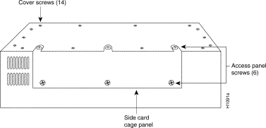
Step 2 If the chassis is rack mounted, disconnect all external cables from the chassis rear panel. Note where these cables were connected, for reinstallation. Step 3 Remove the chassis from the rack and transfer it to a desktop or work table. Step 4 If you need to handle any electronic components (cards, and so forth) attach appropriate ESD protection and attach the AC power cord, but to prevent a shock hazard, make certain the chassis power is OFF. Step 5 To access the cards in the card cage, locate the three flat-blade screws that secure the card cage access panel. (See Figure 8.) These screws are located on the top of the MGS chassis access panel. Step 6 Using the flat-blade screwdriver, turn each of these screws 1/4 to 1/2 turn counterclockwise until the screw pops up. Step 7 Using the No. 2 Phillips screwdriver, loosen the three screws at the bottom edge of the card cage cover. (Do not remove these screws completely.) Carefully remove the card cage cover and set it aside. Step 8 To access the other chassis components, use the No. 1 Phillips screwdriver to remove the 14 screws that secure the top cover of the MGS chassis. (See Figure 8.) Set the top cover aside.
Following is the procedure for accessing the C chassis interior.
Step 2 If you need to handle any electronic components (cards, and so forth) attach appropriate ESD protection and attach the AC power cord, but to prevent a shock hazard, make certain the chassis power is OFF. Step 3 Use the No. 2 Phillips screwdriver to remove the ten screws that secure the cover of the Step 4 Position the chassis so that the back (the side with the ports) is on your left; the front of the chassis (with the LED) is on your right; and the chassis top is facing up. (This is completely opposite of the chassis position shown in Figure 9.) Step 5 Pull the front of the cover to the right (while securing the back of the chassis with your left hand) until the power supply and card cage are completely exposed. Because the fit is snug, pull slowly and carefully, and do not remove the cover.
All CSC/4 cards have ejectors that lock into place when the card is seated in the card cage and allow the card to be extracted easily from its slot. Handle the card as little as possible; try to limit contact to only the ejector tabs and card edges.
Install the CSC/4 card as follows.
Before installing the CSC/4, ensure that you have reviewed the requirements in the section "Installation Prerequisites" on page 7. If you are upgrading from a CSC/1 to a CSC/4 card, be sure to follow the procedure described in the section "Copying and Retrieving the Configuration File" on page 9. Step 2 Turn OFF the power to the chassis. Step 3 Attach an ESD-preventive wrist strap. To channel ESD voltages to ground, make sure the power cable is attached. Step 4 Remove the card access panel (A-type and M chassis) or the cover (C chassis) to gain access to the card cage. (Refer to the section "Opening the Chassis" on page 10.) Step 5 Locate the existing processor card, if any. This card will be either a CSC/1, CSC/2, or a CSC/3 you are replacing, or a CSC/4 if you are upgrading the system software or replacing a bad CSC/4. The processor card is in the top slot in any chassis except an AGS+; where the processor card is in the second slot from the top. (See Figure 10.) Step 6 Disconnect the console/auxiliary port ribbon cable from the front of the existing processor card. Step 7 Remove the processor card. Place the removed card on an antistatic mat or antistatic foam. Step 8 If you are upgrading the system software on an existing CSC/4 card, perform the steps in the section "EPROM Component Replacement" on page 17 before proceeding. Step 9 Check the jumper settings. On new cards, the jumpers are set at the factory for correct operation. You may need to change the settings of jumpers W51 through W53 for system software upgrades.
Figure 6 illustrates the jumper settings to use with each EPROM type by size. The orientation of the jumpers is with the card positioned as shown in Figure 12: component side up with the console cable connector closest to you.
In the following step, failure to place the CSC/4 card in the correct slot prevents correct operation of your system. Step 10 Hold the CSC/4 card by the ejector tabs and the card edges, component-side up, with the bus edge away from you, and insert it in the card cage in the second slot from the top of the card cage.
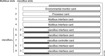
If you are installing the card in an M or C chassis in which the top slot is empty, place the CSC/4 in the top slot. As an example of placement in a card cage, an AGS+ card cage is shown in Figure 10.
Correct card placement order in the card cage is crucial for system functionality. In all systems except an AGS+, memory boards (if any) must be installed in the top cage slot (except the CSC-MC and CSC-MC+, which attach to the bottom of the M and C chassis or the top of the card cage in the AGS+), and the CSC/4 processor card is installed in the slot below it. All other Multibus master cards (CSC-R and CSC-P) must be placed consecutively immediately below the processor card. These are then followed by the other interface cards (MCI, SCI, Ethernet). If you are installing the CSC/4 in a system other than an AGS+, the first (top) slot in the bus may be empty. If so, install the CSC/4 in the top slot. Step 11 Place your thumbs on the ejector tabs and push the card in firmly until it snaps in to place and is firmly seated in the slot. The ejectors close automatically when the card is seated properly. Step 12 Internally, route the ribbon cable from the console port (which is installed in the rear panel of the chassis) over the top of the system card cage and down to the console port on the CSC/4 card. This same cable connects the optional auxiliary port (if any) to the CSC/4 card. Step 13 If you replaced a CSC/2 with a CSC/4, you must change a PAL component on each CSC-MCI and CSC-SCI in your system. Follow the instructions in the section "CSC-MCI and CSC-SCI Modifications" on page 18 before closing the chassis. Step 14 Turn ON power to the system for an installation check, which is described in the following section. When the installation checks out successfully, replace the chassis cover and reboot the system. Note If you upgraded your CSC/1 or CSC/2 to a CSC/4, follow the steps in the section
"Copying and Retrieving the
Configuration File" on page 9, to
retrieve your configuration file.
Following is the procedure for checking out the installation.
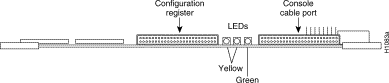
To the right of the configuration register, on the front edge of the processor card, are three LEDs. The left and center LEDs are yellow. (See Figure 11.) The third LED (far right) is green. The LED on the left is a software-programmable status light; it is ON (momentarily) during initialization, flashes to indicate an error, and remains off under normal operation. The middle LED is the processor halt light; it is ON when the processor halts for any reason. This LED can flash at power-up, but should not remain lit; a problem is indicated when it does. The green LED on the right is a software-programmable run light that is ON when the system is running properly.
Note If you power up a system when one or more of the EPROMs is incorrectly inserted, the system
may either halt, and the yellow halt LED will come on, or the system may print a message on the
console reporting an error. When this happens, locate the offending EPROM, straighten the pin, then
reinsert the EPROM and try again. If an EPROM is inserted backwards when power is turned on, the
EPROM will be damaged and must be replaced.
Step 2 If the LEDs display any error conditions, check that all cards are firmly seated.
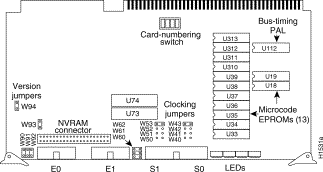
Software for each system is distributed in the form of erasable programmable read-only memory (EPROM) components. Use the following instructions to remove EPROMs from your CSC/4 card and replace them with EPROMs containing upgraded software.
The correct placement of each EPROM is crucial. If improperly positioned, the EPROM will be damaged when the system is powered on. It is imperative that you read through all of the instructions before proceeding. Also, to prevent damage to the EPROMs from electrostatic discharge, be sure to follow the ESD procedures described earlier when handling the cards and their components.
If the software comes in a set of four EPROMs, the EPROMs are inserted into the even-numbered sockets (U42, U44, U46, and U48 only).
If the software comes in a set of eight EPROMs, the EPROMs are inserted into all eight sockets.
The EPROMs are labeled with the appropriate socket (or U) number. The sockets have labels too (although obscure), which are silkscreened on the processor card.
Each EPROM has a notch cut on one end to indicate proper orientation. It should be placed so that this notch faces the same direction as the notch in the EPROM socket, as shown in Figure 1. Do not rely on the orientation of the EPROM labels for correct positioning.
Refer to Figure 12 for placement of the components on the CSC/4 processor card.
Follow these steps to upgrade the EPROM in the CSC/4 processor card:
Step 2 Remove the processor card from the card cage following the card removal and replacement procedures described in steps 1 through 7 of the section "Installing the CSC/4 Card" on page 14. Step 3 Referring to Figure 12, position the CSC/4 card as shown and locate the eight EPROMs in sockets U41 through U48. Note the orientation of the notches on the end of each EPROM to aid in inserting the new EPROMs. Do not rely on the orientation of the labels on the new EPROM for correct positioning. Step 4 Use a chip extractor to remove the first EPROM from its socket. If you do not have a chip extractor available, use a small flat-blade screwdriver to gently pry, then remove the EPROM from its socket. Step 5 Install the new EPROM whose number corresponds to the old EPROM you just removed. Observe the correct notch orientation for the new EPROM. Step 6 Repeat Steps 4 and 5 until all new EPROMs are installed. Be careful not to bend or break any of the pins. Use needlenose pliers to straighten a bent pin. If a pin breaks, contact a customer service representative for a replacement. Step 7 If required , reset the EPROM jumpers on the CSC/4 appropriately for your new software version upgrade. Refer to the section "EPROM Jumpers," on page 6.
When you upgrade your system processor card from a CSC/2 to a CSC/4, you must change a programmable-array logic (PAL) component on any CSC-MCI and CSC-SCI cards in the system. If you are upgrading from a CSC/3 processor card, you do not need to change this PAL. The new PAL contains updated bus-timing logic which allows the cards to operate with the faster processor on the CSC/4. The PAL is shipped as part of the CSC/4 processor card upgrade package. The modifications for both cards are described in the following sections.
Note If you have more than one CSC-MCI or CSC-SCI in your system, remove the first one, replace
the PAL on it, then replace it in the chassis and reconnect the cables before removing the next card.
This avoids potential addressing problems caused by cards replaced in the wrong slots or cables that
become crossed.
The bus-timing PAL on the CSC-MCI is in socket U112, which is located on the right rear portion of the card. (See Figure 13.) If the PAL is already Part Number 17-0675 (or later), the CSC-MCI card needs no further modification. If the PAL is Part Number 13/107A or 17-0038, use the following procedure to remove the CSC-MCI from the card cage and replace the PAL:.
Step 2 Remove the card. Use your thumbs to pull the ejector tabs out and away from the card edge to loosen it, and pull the card out of its slot. Place the removed card on an antistatic mat or antistatic foam. (Refer to Figure 13.) Step 3 Locate the bus-timing PAL (old Part Number 17-0038 or 13/107A) at socket position U112. Step 4 Use a chip removal tool or a small flat-blade screwdriver to gently lift the PAL from the socket and set it aside. Step 5 Carefully insert the new PAL chip into the U112 socket, with the notch on the PAL in the same orientation as the notch on the socket. Be careful not to bend or break any of the pins. To straighten out a bent pin, use needlenose pliers. If a pin breaks, contact a customer service representative to obtain a replacement. Step 6 Replace the CSC-MCI in the original card cage slot. Step 7 Place your thumbs on the ejector tabs and push the card in firmly until it snaps in place and is firmly seated in the slot. The ejectors close automatically when the card is seated properly. Step 8 Turn ON the system to check the installation. Refer to the section "Installation Checkout" on page 16.
The bus-timing PAL on the CSC-SCI is in socket U 213, which is located in the upper-right rear portion of the card. (See Figure 14.) If the PAL is already Part Number 17-0675 (or later), the CSC-SCI card needs no further modification. If the PAL is Part Number 13/107A or 17-0038, use the following procedure to remove the CSC-SCI from the card cage and replace the PAL.
Step 2 Remove the card. Use your thumbs to pull the ejector tabs out and away from the card edge to loosen it, and pull the card out of its slot. Place the removed card on an antistatic mat or antistatic foam. (Refer to Figure 14.) Step 3 Locate the bus-timing PAL (old Part Number 17-0038 or 13/107A) at socket position U213. Step 4 Use a chip removal tool or a small flat-blade screwdriver to gently lift the PAL from the socket and set it aside. Step 5 With the notch on the PAL in the same orientation as the notch on the socket, carefully insert the new bus-timing PAL into the U213 socket. Be careful not to bend or break any of the pins. To straighten out a bent pin, use needlenose pliers. If a pin breaks, contact a customer service representative to obtain a replacement. Step 6 Replace the CSC-SCI in the original card cage slot. Step 7 Place your thumbs on the ejector tabs and push the card in firmly until it snaps in to place and is firmly seated in the slot. The ejectors close automatically when the card is seated properly. Step 8 Turn ON the system to check the installation. Refer to the section "Installation Checkout" on page 16.
Setting the Console Port Baud Rate
General Configuration Register Settings
bit 13 causes the system to load operating software from read-only memory (ROM) after five unsuccessful attempts to load a boot file from the network. Clearing bit 13 causes the system to continue attempting to load a boot file from the network indefinitely. By factory default, bit 13 is cleared to 0.
Figure 4 CSC/4Optional Configuration Register Settings
EPROM Jumpers
Figure 5 CSC/4 EPROM Jumper Locations—Partial Component-Side View
Figure 6 CSC/4 EPROM Jumper Settings
Installation Prerequisites
System Compatibility
Required Parts
Required Tools
Preventing Electrostatic Discharge Damage
If the component will be returned to the factory, immediately place it in a static shielding bag.
![]()
Caution Copying and Retrieving the Configuration File
Copying the Configuration File
Step 1 Log onto a TFTP file server and create a temporary file. Most hosts will require that you create the destination file first and that it be "world-writable."
router#
Remote host []?
Name of configuration file to write [router-confg]?
Write file gsxx-confg on host 131.131.101.101?[confirm]
Writing gsxx-confg:!!!! [ok]
Retrieving the Configuration File
Step 1 Upload the configuration file from the TFTP server using the command config net. When prompted, supply the host address of the TFTP server and the file name containing the configuration data. A sample output of the config net command follows:
Installation
Opening the Chassis
Tools Required
A-Type Chassis Access Procedure
![]()
Warning
Step 1 Turn OFF power to the chassis and unplug it from AC power.
Figure 7 Chassis Front and Top Panels
MGS Chassis Access Procedure
Step 1 Turn OFF power to the chassis and unplug it from AC power.
Figure 8 Screw Locations on the MGS Chassis Exterior—Side View
C Chassis Access Procedure
Step 1 Turn OFF power to the chassis and unplug it from AC power.
C chassis. There are two screws on each side and six screws on the bottom of the chassis. (See Figure 9.)
Figure 9 Screw Locations on the C Chassis Exterior—Side View
![]()
Caution
Installing the CSC/4 Card
![]()
Caution
Step 1 Firmly seat the chassis on a stable surface.
![]()
Caution
![]()
Caution
Figure 10 AGS+ System Card Cage
Installation Checkout
Step 1 Turn ON the system power and observe the LEDs on the CSC/4 card.
Figure 11 CSC/4 LED Indicators—Front-Edge View
EPROM Component Replacement
![]()
Caution
Step 1 Turn OFF power to the chassis, then gain access to the card cage. Refer to the procedures in the section "Opening the Chassis" on page 10.
Figure 12 CSC/4Processor Card—Component-Side View
CSC-MCI and CSC-SCI Modifications
Modifying the CSC-MCI
Step 1 Disconnect the serial and/or Ethernet interface cables from the front of the CSC-MCI. (See Figure 13.)
Figure 13 CSC-MCI Card—Component-Side View
Modifying the CSC-SCI
Figure 14 CSC-SCI Card—Component-Side View
Step 1 Disconnect the serial cables from the front of the CSC-SCI.
![]()
![]()
![]()
![]()
![]()
![]()
![]()
![]()
Posted: Thu Nov 6 16:12:40 PST 2003
All contents are Copyright © 1992--2003 Cisco Systems, Inc. All rights reserved.
Important Notices and Privacy Statement.