|
|

Product Numbers: APP-JI1=, APP-LI2=, APP-LI4=, APP-LI6=, APP-LI8=, APP-II1=, APP-SI2=,
APP-SI4=, and CAB-X21CF=
This publication contains instructions for installing the Cisco X.21 dual-mode applique in your router. The applique can function as either a data terminal equipment (DTE) or a data communications equipment (DCE) interface. The default is DTE, but you can change the mode to DCE by changing jumper settings and connecting an optional DCE interface cable, which is available from us. Following is the information included in this publication:
Before beginning installation, read this entire document to ensure that you have all the necessary tools and equipment, and that you have the correct modules for your system configuration.
The term applique refers to the hardware unit that provides the external interface connections from your router to the network. An applique comprises connector-mounting hardware (connector port) and a printed circuit card, which translates communications signals from/into the specified electrical specification (X.21 and so forth). Appliques are mounted on connector plates in the rear of the router chassis. Depending on the applique type and the size of your system, from one to eight appliques can be mounted on a single connector plate. Three plate sizes are available: large, small, and individual. A ribbon cable connects the applique internally to a serial network interface control card.
Figure 1 shows an individual- and a large-size connector plate as they would be installed in an A-type chassis. The small connector plate, which is used in the M chassis, is not shown.
The maximum possible number of connections is determined by connector type, space available in the chassis connector plate areas, and the available ports on the network interface cards (CSC-MCI or CSC-SCI). Table 1 lists the options by product number, for each applique model.
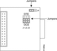
The X.21 applique, which is designed for domestic and international use, meets the CCITT specification for a DTE, VDE Class B, and FCC Class A, CSA C108.8. The applique can be set for either DTE or DCE mode, with default mode as DTE. Change the mode to DCE by changing the position of jumpers J1, J2, and J3. (See Figure 2.) All three jumpers must be in the same position (DCE or DTE) in order for the applique to operate properly. Jumper J4 connects logic ground to chassis ground when in the default position. (See Figure 2.) Special DTE and DCE cables are required for DTE or DCE operation. Table 2 lists the pinout for the dual-mode X.21 applique.
|
| 1 These signals go to the DCE device only when the jumpers are set for DCE, and the DCE transition cable is used. |
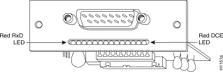
On the X.21 serial applique, the 14 LEDs, which are positioned as shown in Figure 3, indicate the status of the interface. Use the green LEDs toward the end of the row for orientation. The LEDs are located beneath the connector. The LEDs are listed in Table 3 as viewed from left to right when facing the front of the applique, as shown in Figure 3.
Table 3 X.21 Applique LED Indicators
|
| 1 Loopback is available in DCE mode only. |
The X.21 applique is used with either the CSC-MCI or CSC-SCI network interface cards. Both cards are shipped with the factory default set to work with DTE appliques. When using a DCE applique, all versions of the SCI card are compatible; however, MCI cards must be running Microcode
Version 1.5 or later for the DCE clocking mechanism to work correctly. In addition, the clock source jumpers on the MCI or SCI cards must be properly positioned, as described following.
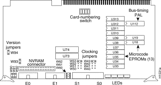
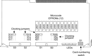
The MCI card is shown in Figure 4. The SCI card is shown in Figure 5. The orientation of both cards is component side up, with the interface cable connector edge at the bottom of the card.
The CSC-MCI and CSC-SCI cards ship with the factory default set to work with data terminal equipment (DTE) appliques. Therefore, you may need to change jumper settings on your MCI or SCI card for it to operate with a data communications equipment (DCE) applique, or to reset the clock source options.
DTE appliques require external clocking; the customer service unit/data service unit (CSU/DSU) provides the clocking for the circuit. Attaching an X.21 applique to a modem or CSU/DSU almost always requires DTE format. DCE appliques receive internal clock signals from the MCI or SCI interface card.
On the MCI card, jumpers W51 and W41 control the serial ports 0 and 1 in data communications equipment (DCE) mode. On the SCI card, jumpers N22, N26, N12, and N16 control the serial ports 0 through 3 in DCE mode. In addition to changing these jumpers for DCE operation, you must configure the clock rate on each serial interface of the interface card using the clockrate speed interface subcommand (where speed is the bit rate of the interface in bits per second [bps]). The applique must be DCE (or configured as DCE) to generate the clock signals.
Following is sample output of the clockrate speed command:
The no clockrate command removes the clock rate if data terminal equipment (DTE) mode is desired. Refer to the appropriate configuration and reference publication for more information on these commands. Following are the acceptable clockrate speed settings, appearing as they are entered with the clockrate speed command:
1200, 2400, 4800, 9600, 19200, 38400, 56000, 6400, 7200, 12500, 148000, 500000, 800000, 1000000, 1300000, 2000000, and 4000000
The fastest speeds might not work if your cable is too long. Speeds faster than 148 kilobits per second (kbps) are not recommended for RS-232 or RS-232 SDLC signaling. It is recommended that you use the RS-232 and SDLC appliques only at speeds up to 64 kbps; for speeds above this, use RS-449, X.21, or HD V.35.
Most DTE interfaces require a Normal External Transmit Clock signal. All DCE interfaces require an Internal Transmit Clock (noninverted) signal. The MCI card clocking options are controlled by jumper areas W40 through W53, and the SCI card clocking options are controlled by jumper areas N11 through N28.
Occasionally, delays occur between the Serial Clock Transmit External (SCTE) clock and the transmitted data that may push the data transition out to the point where using an inverted clock is appropriate (jumpers W42 and W52 for the MCI and N13, N17, N23, and N27 for the SCI); however, an inverted clock is not recommended.
Typical delays indicate that the inverted clock may be appropriate above 1.3 megabits per
second (Mbps), depending upon the DTE clock-to-data skews and setup required, and allowing some margin for temperature, cable, and other variables. Some DCE devices will not accept SCTE, so Serial Clock Transmit (SCT) must be used. Inverting the clock may be the only way to compensate for the cable length and circuit delays in the DTE and DCE.
Table 4 and Table 5 show the jumper settings for the MCI and SCI clock options, respectively. The last two columns of these tables (DTE and DCE) indicate the setting that should be used with either a DTE or DCE applique. Unless specifically noted, all products are shipped with the factory default setting to work with the DTE applique, which requires external clocking; the channel service unit/digital service unit (CSU/DSU) provides the clocking for the circuit.
Table 4 CSC-MCI Jumper Settings for Clock Options
|
| 1 X = Recommended setting. x = Available but not recommended. |
Table 5 CSC-SCI Jumper Settings for Clock Options
|
| 1 X = Recommended setting. x = Available but not recommended. |
Before installing the applique, ensure that your system meets the following prerequisites:
Verify that you have all of the following parts:
Electrostatic discharge (ESD) is a discharge of stored static electricity that can damage equipment and impair electrical circuitry. It occurs when electronic components are improperly handled and can result in complete or intermittent failures. Following are guidelines for preventing ESD damage:
| Caution For safety, periodically check the resistance value of the antistatic strap. The measurement should be within the range of 1 and 10 Mohms. |
Choose the following procedure that describes your chassis type.
Following is the procedure for accessing the A-type chassis interior. This procedure requires a medium-sized flat-blade screwdriver.
| Warning Before accessing the chassis interior, turn OFF power to the chassis and unplug the power cord because hazardous voltages may exist in or near the power supply. Use extreme caution when working near the power supply. |
Step 2 If the chassis is rack mounted, disconnect all external cables from the chassis rear panel. Note where these cables were connected, for reinstallation.
Step 3 Remove the chassis from the rack and transfer it to a desktop or work table.
Step 4 If you will need to handle any electronic components (cards, and so forth), attach appropriate ESD protection and attach the AC power cord, but to prevent a shock hazard, make certain the chassis power is OFF.
Step 5 To access cards in the card cage, loosen the two thumbscrews and remove the front panel from the chassis. (See Figure 6.) If you wish to access cards in the card cage only, skip the next step.
Step 6 To access other system components, locate and remove the seven No. 1 Phillips screws securing the top cover. (See Figure 6.) Set the top cover and screws aside.
To reassemble the chassis, reverse all steps.
Following is the procedure for accessing the MGS chassis interior. You will need a medium-sized flat-blade screwdriver and No. 1 and No.2 Phillips screwdrivers.
Step 2 If the chassis is rack mounted, disconnect all external cables from the chassis rear panel. Note where these cables were connected, for reinstallation.
Step 3 Remove the chassis from the rack and transfer it to a desktop or work table.
Step 4 If you need to handle any electronic components (cards, and so forth) attach appropriate ESD protection and attach the AC power cord, but to prevent a shock hazard, make certain the chassis power is OFF.
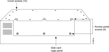
Step 5 To access the cards in the card cage, locate the three flat-blade screws that secure the card cage access panel. (See Figure 7.) These screws are located on the top of the MGS chassis access panel.
Step 6 Using the flat-blade screwdriver, turn each of these screws 1/4 to 1/2 turn counterclockwise until the screw pops up.
Step 7 Using the No. 2 Phillips screwdriver, loosen the three screws at the bottom edge of the card cage cover. (Do not remove these screws completely.) Carefully remove the card cage cover and set it aside.
Step 8 To access the other chassis components, use the No. 1 Phillips screwdriver to remove the 14 screws that secure the top cover of the MGS chassis. (See Figure 7.) Set the top cover aside.
To reassemble the chassis, reverse all steps.
Following is the procedure for accessing the C chassis interior. You will need a medium-sized flat-blade screwdriver and No. 1 and No. 2 Phillips screwdrivers.
Step 2 If you need to handle any electronic components (cards, and so forth) attach appropriate ESD protection and attach the AC power cord, but to prevent a shock hazard, make certain the chassis power is OFF.
Step 3 Use the No. 2 Phillips screwdriver to remove the ten screws that secure the cover of the
C chassis. There are two screws on each side and six screws on the bottom of the chassis. (See Figure 8.)
Step 4 Position the chassis so that the back (the side with the ports) is on your left; the front of the chassis (with the LED) is on your right; and the chassis top is facing up. (This is completely opposite of the chassis position shown in Figure 8.)
Step 5 Pull the front of the cover to the right (while securing the back of the chassis with your left hand) until the power supply and card cage are completely exposed. Because the fit is snug, pull slowly and carefully, and do not remove the cover.
| Caution Several cables are located close to the interior of the C chassis cover. Avoid damage to these cables by ensuring that they do not impede the cover as you remove it. |
To reassemble the chassis, reverse all steps.
The X.21 applique is already mounted on a connector plate. If you are installing a new interface, you need only install the new plate as described in the procedure "Installing the Connector Plate." If you are replacing existing RS-449 appliques, you also must perform the steps in the following procedure "Replacing an Existing Connector Plate."
When replacing RS-449 appliques, you can use the existing internal ribbon cables with the new X.21 applique. Disconnect the cables from the RS-449 appliques, but do not disconnect them from the MCI or SCI cards. When disconnecting more than one RS-449 applique, tag the internal ribbon cable of each one before disconnecting the next; this will help avoid crossing the internal cables and mixing up your designated interfaces.
The following procedure describes the steps for removing an existing RS-449 applique plate. If you are not replacing existing connectors, skip this section and proceed to the following section "Installing the Connector Plate."
Step 2 Disconnect all external interface cables from the connector plate you are replacing.
Step 3 Disconnect each ribbon cable from the connector on the RS-449 applique. Tag each cable as you disconnect it to avoid confusing it later. Do not disconnect the ribbon cable from the MCI or SCI card.
Step 4 On the rear of the chassis, loosen and remove the Phillips screws that secure the connector plate to the chassis. Individual plates are secured with two screws, small plates with four screws, and large plates with six screws.
Step 5 Carefully lift the plate up and out of the chassis, without straining any internal cables.
Step 6 To complete the installation, proceed to the next section, "Installing the Connector Plate."
The following procedure describes how to install the new connector plate. While performing these steps, refer to Figure 1, which illustrates the location of connector plates on the chassis.
Step 2 Ensure that all applique jumpers are set correctly. Refer to the section "LED Indicators" on page 4.
Step 3 On the rear of the chassis, remove a blank connector plate from the connector area.
Step 4 Place the new connector plate, with the attached X.21 applique, on the inside of the chassis against the opening.
Step 5 Position the applique with the X.21 connector facing out and the LEDs above the connector.
Step 6 Secure the applique with the screws you removed from the blank (or RS-449) connector plate.
Step 7 Connect an internal ribbon cable to the 26-pin connector on each applique.
If the cables are not already connected to the MCI or SCI interface cards, route the cable under the system card cage and up to a serial connector on the card. Attach the cable to the first available serial connector on either card. Be careful not to strain or crimp the cable.
Step 8 Plug an appropriate interface cable from your network segment into the X.21 connector on the applique. If you changed your applique to operate in DCE mode, install the cable with the "DCE" label at the network connection end.
Step 9 Turn ON power to the system to check the installation as described in the following section.
After you have installed your applique, verify that it is installed correctly before you replace the cover. Turn the system power on and observe the status indicators on the applique and the interface card, then use EXEC show commands to verify that your interfaces are recognized by the system and have been assigned port addresses.
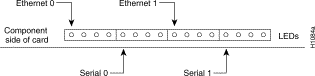
The CSC-MCI and CSC-SCI cards contain a bank of 16 LEDs. (Four are currently used.) Table 6 lists the LEDs that are used and the serial and Ethernet port each LED represents. LED 0 is at the left end of each block of four LEDs (as you view the front edge of the card in the system card cage, as shown in Figure 9 and Figure 10).
At startup, all LEDs flash and then only those LEDs that indicate active interfaces will stay on. A problem is indicated if all LEDs remain on after the system boots, or if the LED of a specific interface does not stay on after the system boots.
Table 6 CSC-MCI and CSC-SCI LED Indicators
When the indicated LED is lit, Carrier Detect (CD) is present on that serial interface, and the interface is enabled. In Ethernet systems, this means that the interface is attached to the Multibus correctly, but is not an indication of complete functionality.
A problem is indicated if an LED is not on, but the interface to which it corresponds is connected, or if all LEDs are on after start up, but not all interfaces are in use.
When the LED indicators show that the applique is installed correctly, use the EXEC command show controller mci to display the current internal status of the MCI and SCI cards, including the interfaces and how the card has identified them. Although the command specifies the MCI card, it also provides the same information for SCI cards; controller types 1.0 and 1.1 are MCI cards, and controller type 2.0 is an SCI card. The display lists all interfaces connected to the MCI and SCI cards, including Ethernet interfaces on the MCI cards. The display indicates that the system has identified your new interface, but it does not indicate the state of the line or protocol.
Following is sample output for a system with three serial and one Ethernet interfaces:
To obtain more extensive information about the interfaces, such as the state of the lines and protocol types, use the EXEC command show interface type unit (where type is the interface type, and unit is the interface unit address) to display statistics about each of the interfaces in the server. You can also use the command show interface (without variables) to display all network interfaces. Each new serial interface should be appended to the list of existing interfaces, with the next sequential number assigned to it.
In the following example, one new serial interface (serial 2) was added to two existing serial interfaces:
Much more information is displayed than what is shown in this example.
When the installation check is successful:
Step 2 Replace and secure the chassis cover.
Step 3 Affix the new labels (Serial 0, Serial 1) below the connector on the rear of the chassis.
Step 4 Turn ON power to the system to configure your network interface.
The router products configuration publication contains additional information for configuring the new interface and managing the system.
![]()
![]()
![]()
![]()
![]()
![]()
![]()
![]()
Posted: Thu Nov 6 16:11:27 PST 2003
All contents are Copyright © 1992--2003 Cisco Systems, Inc. All rights reserved.
Important Notices and Privacy Statement.