|
|

An MGX 8260 media gateway consists of the following hardware components:
This subsection briefly describes the hardware components and their interconnections.
The MGX 8260 chassis is a rack mountable cabinet with 16 card slots, a midplane, an integrated fan unit and -48VDC power distribution network. The chassis is New Equipment Building System (NEBS) Level 3 certified for use in carrier environments. It can be mounted in a 19-in. or 23-in. equipment rack using the rack mount ears supplied with the MGX 8260. The mounting ears can be positioned for flush or offset mounting in telco equipment racks and cabinets. (See Figure 2-1.)
Two of the 16 slots are designated to support primary and redundant System Control Cards (SCCs). The other slots accept a variety of service circuit front and back cards.

| 1 | Chassis—Front View | 2 | Chassis—Back View |
| 3 | Air plenum | 4 | |
| 5 | Air intake panel | 6 | Input power and grounding terminals |
| 7 | Air deflector panel | 8 |
The chassis incorporates a midplane which accepts plug-in cards from the front and rear of the chassis. (See Figure 2-2.) The midplane contains the communication and power buses which support interprocess and data communication among circuit cards. It also deflects air flow through the front cards and out the top of the chassis.
A variety of sensors throughout the chassis and circuit cards monitor temperature and voltage. This environmental data is routed to and processed by the active SCC. Environmental data outside acceptable limits triggers an alarm condition and writes an error message to the log file. Network Management Systems can receive simple network management protocol (SNMP) traps whenever an environmental parameter is exceeded.
Air is drawn through the intake vent at the bottom of the chassis by a series of fans at the top of the chassis. (See Figure 2-2.) The fan unit contains three hot swappable fan trays. Each tray holds two fans for a total of six fans in the chassis. The MGX 8260 can function with four of the six fans operational.
The fans draw the intake air through the circuit cards. Without the air plenum the warmed air exhausts directly through the top of the chassis. The plenum contains a baffle which deflects the warmed air towards the back and sides of the chassis. The plenum must always be installed if the MGX 8260 is not at the very top of the equipment rack.
Sensors in the fan trays monitor the rotational speed of the fans as well as ambient temperature. Each fan is identified by a unique number based on its location. The identifier appears in alarm messages when a faulty fan is detected. (Refer toTable 2-1.)
| Tray | Front | Rear |
|---|---|---|
Tray 1 (left) | Fan 1 | Fan 2 |
Tray 2 (center) | Fan 3 | Fan 4 |
Tray 3 (right) | Fan 5 | Fan 6 |
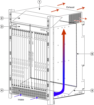
| 1 | Air plenum | 2 | Deflector plate - plenum |
| 3 | Fan unit | 4 | Air intake panel |
| 5 | Deflector plate - internal | 6 | Midplane |
The MGX 8260 chassis accepts -48 VDC power from two separate sources—Feed A and Feed B. Power connections are made at the bottom rear of the chassis (see Figure 2-1, Item 6). The input feeds are routed via the midplane to the front cards. Each front card incorporates DC-to-DC power converters which supply the individual voltages required on each card.
The MGX 8260 chassis incorporates two ground points at the bottom rear of the chassis (see Figure 2-1, Item 6). During the installation process, one of the ground points should be tied to the building ground point via a heavy conductor and two-hole ground lug.
Physical card slots are numbered 1 through 16 starting from the left-front of the chassis. Slots 9 and 10 only accommodate the double-wide SCCs. When provisioned in the chassis, Distribution Matrix Cards (DMCs) can only be installed in slots 7 and 8. Broadband Service Cards (BSCs) are restricted to slots 11 through 16. Narrowband Service Cards (NSCs) can be installed in slots 1 through 8 and 11 through 16.
 |
Note Empty card slots should always be covered by blank panels to sustain air flow and minimize the potential for electromagnetic interference (EMI). |
DMCs, BSCs and NSCs are collectively known as service circuit cards. This subsection briefly describes the features and functions of each type of front card.
The System Control Card (SCC) provides the switching and management interface for the MGX 8260. Designed for carrier environments, with no single point of failure in a redundant configuration, calls in progress are maintained even if the SCC or service cards fail. The SCC provides a 5 Gbps switching fabric for the chassis. Figure 2-3 shows a simple block diagram of the SCC. Each subcomponent is briefly described below.

The central processing unit (CPU) maintains and executes the system functions of the MGX 8260. An R5000 type, 64-bit RISC processor serves as the CPU operating at an internal clock speed of 266 MHz and an external clock speed of 66.66 MHz.
An associated host bridge/memory controller handles SDRAM memory and provides device control via two independent 32-bit PCI interfaces. It also incorporates four DMA channels to transfer data between PCI ports on its dual PCI buses, its local SDRAM and input/output slave device.
The dual PCI interfaces operate at 33 MHz. PCI Bus A interfaces to an integrated SAR controller and an external BIM slot. PCI Bus B interfaces to two 10/100 Ethernet management ports and the PCI IDE controller.
Local data/program memory/packet buffer memory is stored on a 256 MB SDRAM module. SDRAM serves as the primary volatile memory system. It also "shadows" the flash memory so that performance is enhanced when running program memory.
Flash memory (2 MB) is used for boot strapping the CPU. The boot-up section is only 16 bits wide.
The CSM outputs 8 KHz and 192 KHz clock signals referenced by other devices. It also provide the following clocks to subsystems:
The broadband interface module (BIM) is a daughter card that provides Fast Ethernet (FE) or OC-3 interface capabilities. The BIM type (FE or OC-3) must match the back card type (SCCBC-4FE or OC3SMIBC) for proper SCC operation. A label on the SCC front card identifies whether it is equipped with the FE or OC-3 BIM.
An erasable programmable logic device (EPLD) serves as the controller and handles the signaling handshakes between the SCC and DMC.
The Cell Bus interface consists of a SAR controller and bus interface circuitry.
The ATMizer II scheduler block supports six levels of traffic priorities. The scheduler unit supports four independent calendar tables and performs traffic management functions on a large number of connections with arbitrary cell rates.
For additional processing flexibility, an enhanced direct memory access (DMA) controller performs the AAL5 SAR function in hardware. The ATMizer II+ device provides a 32-bit, 33 MHz PCI V-2.1 compliant bus interface for host access and a 32-bit 80 MHz local memory interface for data and control structures, and an 8-bit 50-MHz UTOPIA level-2 compliant port for PHY (OSI Layer 1) interface.
The Cell Bus interface consists of dual VLSI chips that implement ATM multiplexing and switching based on the Cell Bus architecture. The VLSI chip supports unicast and multicast transfers, cell address translation, cell routing and outlet cell queuing. Ingress and egress field programmable gate arrays (FPGAs) with custom application specific integrated circuits (ASICs) control ATM data cell transfer across the dual Cell Buses.
The ATM switch fabric section consists of the following components:
SCC front cards and back cards are mated based on the BIM installed on the front card. The SCC front card label identifies whether an FE or OC-3 BIM is installed. The FE BIM requires the SCCBC-4FE back card; the OC-3 BIM requires the OC3SMIBC (single mode fiber) back card. In redundant configurations, the SCC front cards and back cards must be matched pairs. Figure 2-4 identifies the SCC front and back cards.
The OCSMIBC back card uses LC type fiber connectors for single mode fiber interfaces.
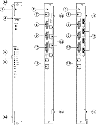
| 1 | SCC front card | 2 | SCCBC-4FE back card |
| 3 | OC3SMIBC or OC3MMIBC back card | 4 | SCC front card label |
| 5 | Clear reset button | 6 | ACO reset button |
| 7 | 8 | Console port—serial DB9, female | |
| 9 | Auxiliary port—serial, modem [DB9, female] | 10 | Alarm connector—DB15, female |
| 11 | Ethernet management ports—10BaseT [RJ45] | 12 | Fast Ethernet ports - 100BaseTx [RJ45] |
| 13 | OC-3 single mode fiber interface connectors | 14 | Front card extractor lever |
| 15 | Back card extractor lever |
|
The SCC front card incorporates a number of status LEDs on its front panel. Figure 2-5 shows the LEDs and their labels. Table 2-2 lists the operational states associated with each LED.

| Classification/Label | Color | State | Description |
|---|---|---|---|
BIM Interfaces | - | - | Indicates current state of the four BIM ports—FE or OC-3—going to the SCC back card. |
FDX | Green | On | Steadily illuminates to indicate full duplex communication with back card port. |
| Green | Off | Indicates half duplex communication with back card port. |
| Red | Off | Steadily illuminates to indicate port failed condition. |
ACT | Green | On/Flash | Illuminates when Ethernet signal has been detected. Flashes to indicate data transfer activity on the port. |
Ethernet Mgmt Ports | - | - | Indicates current state of the two 10BaseT node management ports—LAN 1, LAN 2. |
LINE | Green | On | Steadily illuminates to indicate end point to end point communication with network device. |
ACT | Green | Flash | Flashes to indicate data transfer activity on the port. |
Alarm Status | - | - | Indicates current alarm state of this MGX 8260 node. |
ALMC (Chassis Alarm) | Red | On | Illuminates steadily to indicate that a major alarm condition currently exists. |
| Yellow | On | Illuminates steadily to indicate that a minor alarm condition currently exists. |
| Green | On | Illuminates steadily to indicate that no alarm condition currently exists. |
ALMH (Alarm History) | Red | On | Illuminates steadily to indicate that a major chassis alarm has been detected since the CLR button was pressed. |
- | - | Press these momentary contact buttons to clear existing alarms to an external monitoring system or reset the alarm history indicator. Insert a stiff wire (a bent paper clip will do) and press inward and release to trigger the reset operation. | |
CLR | - | - | Extinguishes the ALMH LED. |
ACO | - | - | Deactivates the alarm relay contacts feeding the Alarm connector on the SCC back card. Any new alarm will reactivate the relay contacts. |
Disk | - | - | Indicates current operating status of the 220MB flash disk. |
| Red | On | Illuminates steadily to indicate flash disk cannot be accessed. |
| Green | Off/Flash | This LED remains extinguished when the disk is available but is not being accessed. It flashes when the disk is accessed for data transfer. |
Power Feeds | - | - | Indicates the state of the -48VDC power feeds to the MGX 8260 chassis. |
PWR A (DC Feed A) | Green | On | Illuminates steadily to indicate that Feed A is supplying nominal voltage to the chassis. |
| Yellow | On | Illuminates steadily to indicate that Feed A is supplying voltage outside the nominal range to the chassis. |
| Red | On | Illuminates steadily to indicate that Feed A is supplying voltage outside the acceptable range to the chassis. |
| - | Off | This LED is extinguished when no power is being supplied to the chassis from Feed A. |
PWR B(DC Feed B) | Green | On | Illuminates steadily to indicate that Feed B is supplying nominal voltage to the chassis. |
| Yellow | On | Illuminates steadily to indicate that Feed B is supplying voltage outside the nominal range to the chassis. |
| Red | On | Illuminates steadily to indicate that Feed B is supplying voltage outside the acceptable range to the chassis. |
| - | Off | This LED is extinguished when no power is being supplied to the chassis from Feed B. |
Card | Green | On | Illuminates steadily to indicate that the SCC is in Active mode. |
| Yellow | On | Illuminates steadily to indicate that the SCC is in Standby mode. |
| Red | On | Illuminates steadily to indicate that the SCC has failed. |
FE or OC-3 Interfaces | - | - | Indicate the current state of the four FE media drops or OC-3 fiber links connected to the SCC back card. |
| Green | On | Illuminates steadily to indicate that the interface is active and no alarms have been detected. |
| Yellow | On | Illuminates steadily to indicate that an alarm condition has been detected on the interface. |
| Red | On | Illuminates steadily to indicate that interface is no longer handling data communication. |
| - | Off | This LED is extinguished when the FE or OC-3 interface has not been configured in the MGX 8260 database. |
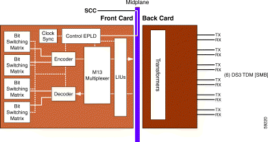
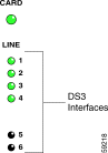
The DMC serves as an M13 multiplexer between DS3 streams and NSCs. The DS1s are demultiplexed from the DS3 stream and mapped to an NSC via a hybrid TDM midplane. The back card provides connections for six DS3 trunks via SMB connectors.
Figure 2-6 shows a simple block diagram of the DMC. Each subcomponent is briefly described below.
The line interface unit (LIU) uses separate line transmitters and receivers for each of six DS3 interfaces. The LIUs contain a built-in B3ZS line encoder-decoder. B3ZS encoded data from the ingress DS3 interface is applied to the M13 multiplexer. For DS3 egress separate DS3 transmit clock and data signals are accepted from the M13 multiplexer, with B3ZS encoding performed before sending the digital stream to the DS3 interface.
The receive and transmit DS3 line terminations are provided on the front card. The back card incorporates isolation transformers and the physical interfaces for connecting 75-ohm coaxial cables.
Ingress data flows from the receive LIU to the M13 multiplexer. The incoming DS3 stream is demultiplexed into 28 separate DS1 streams. Separate data and clock signals are fed to the encoder FPGA block sitting downstream. For egress operations, M13 multiplexer receives clock and data signals for 28 separate DS1 streams from the decoder FPGA block and multiplexes them into a single DS3 stream. The DS3 stream is fed to the LIU transmit interface.
The encoder/decoder block uses a proprietary methodology to encode two separate clock and data streams into one stream before giving it to the midplane and vice versa decodes the encoded stream from the midplane into separate TDM clock and data signals. Six FPGAs implement six independent encoder/decoder blocks. Each FPGA block supports encoding and decoding for 28 T1 streams contained in a single DS3. Thus each block supports the encoding/decoding functions for individual DS3s.
The crossbar switch matrix uses bit switching devices to impart any-by-any switching capability to the DMC. The whole switch matrix is subdivided into two ingress and egress sections, corresponding to each direction of data flow on DS3 line interface. Each sub-section uses two switching devices.
For ingress operation the 168 T1 streams demultiplexed from six DS3s enter as a single signal per T1 stream from the encoder block. In the same direction, the output of the switch matrix is connected to 192 streams routing to various midplane slots supporting NSCs on the MGX 8260 chassis.
In the egress direction, the 192 encoded streams coming from midplane are taken directly (after buffering), to the egress section of the switch matrix. All 192 inputs are copied to both the switching devices used in this block. The 168 output streams from this block are connected to the decoder block.
This distribution of inputs and outputs enables firmware to cross-connect any TDM stream from a DS3 to any TDM stream going to the midplane while avoiding contention between device outputs.
An erasable programmable logic device (EPLD) serves as the controller and handles the signaling handshakes between the SCC and DMC.
The DMC synchronizes the transmit DS3 clocks to the 8-KHz reference provided by the SCC through the midplane. In the receive direction, the DMC can supply 8-KHz reference to the midplane or derive clock synchronization through the channelized DS3.
The DMC generates a 44.736 MHz clock to be used as the transmit clock for the DS3 interfaces. The clock generator is a phase locked loop (PLL) synthesizer which accepts an 8KHz clock signal as an input reference.
The DMC is also capable of supplying two separate 8-KHz references to the midplane as primary and secondary reference clocks. The source for each of these references is selectable individually from any of the incoming six DS3 streams. Each of these reference clock signals has an individual tri-state control.
The DMC incorporates two temperature sensors.
The DMC supports local line, remote line and DS3 metallic loop backs for various diagnostics and debugging purposes.
The DMC front card always uses the T3E3DC-6DSC back card which supports six DS3 interfaces. In redundant configurations, there are always two DMCs and two SCCs in the MGX 8260 chassis. Y-cables split the transmit and receive cables from each DS3 trunk across the two identically configured DMCs. Figure 2-7 identifies the DMC front and back card.

| 1 | DMC front card | 2 | T3E3DC-6DSC back card |
| 3 | DS3 transmit and receive connectors [SMB] | 4 | Diagnostic port [DB9, female] |
| 5 | Front card extractor lever | 6 | Back card extractor lever |
The DMC front card incorporates a number of status LEDs on its front panel. Figure 2-8 shows the LEDs and their labels. Table 2-3 lists the operational states associated with each LED.
| Classification/Label | Color | State | Description |
|---|---|---|---|
Card | Green | On | Illuminates steadily to indicate that the DMC is in Active mode. |
| Yellow | On | Illuminates steadily to indicate that the DMC is in Standby mode. |
| Red | On | Illuminates steadily to indicate that the DMC has failed. |
Line 1-6 | Green | On | Illuminates steadily to indicate that the DS3 interface is active and no alarms have been detected. |
| Yellow | On | Illuminates steadily to indicate that an alarm condition has been detected on the DS3 interface. |
| Red | On | Illuminates steadily to indicate that the DS3 interface is no longer handling data communication. |
| - | Off | This LED is extinguished when the DS3 interface has not been configured in the MGX 8260 database. |
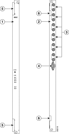
The Broadband Service Card (BSC) supports DS3 (T3) connections and TDM switching functionality. This card, unlike the DMC, is a full 3/1/0 multiplexer and does not require NSCs to terminate the T1s. Each BSC supports up to six DS3s and can be used in a 1:1 redundant configuration. This card is currently restricted to slots 11-16 in the MGX 8260 chassis (a maximum of six BSCs per node).
Figure 2-9 shows a simple block diagram of the BSC. Each subcomponent is briefly described below.
The central processing unit (CPU) maintains and executes the broadband interface functions of the BSC. An R5000 type, 64-bit RISC processor serves as the CPU operating at an internal clock speed of
266 MHz and an external clock speed of 66.66 MHz.
An associated host bridge/memory controller handles SDRAM memory and provides device control via two independent 32-bit PCI interfaces. It also incorporates four DMA channels to transfer data between PCI ports on its dual PCI buses, its local SDRAM, and an input/output slave device.
The dual PCI interfaces operate at 33 MHz and interface to integrated SAR and HDLC controllers, as well as the switch port fabric.
Local data/program memory/packet buffer memory is stored on a 256 MB SDRAM module. SDRAM serves as the primary volatile memory system. It also "shadows" the Flash memory so that system performance is enhanced.
Flash memory (2MB) is used for boot strapping the CPU. The boot-up section is only 16-bits wide.
The hardwired SAR functionality is optimized for AAL5 traffic. Connections with different quality of service (QoS) parameter values are efficiently scheduled and serviced via an integrated hardware scheduler that supports up to four priority classes. The scheduler uses calendar tables to create arbitrary traffic schemes to a limit of 64K virtual connections.
The device's memory controller provides a glueless interface with synchronous DRAMs that are used for local memory, while also serving as a control interface for external physical layer devices.
The primary interface for the device is a 33 MHz, 32-bit wide PCI bus. As the bus master, the ATMizer is able to autonomously access control and data structures in system memory. As a bus slave, the device provides transparent access to local memory and to the internal cell buffer for external PCI bus masters. The PCI interface also implements four separate first in/first out (FIFO) buffers to maximize the performance of simultaneous read/write operations as bus master or slave.
The ATMizer uses 16 MB of SDRAM as its program and data memory. For maintaining configuration and control tables, 512 KB of SSRAM is provided.
The ATMizer's PCI bus runs at 33 MHz whereas the core CPU runs at 40 MHz via an independent oscillator.
The BSC's switch port fabric does the following:
The AAL1 SAR called AAL1gator II performs the following tasks:
The M13 multiplexer has a glueless interface to the LIUs and is capable of supporting asynchronous multiplexing and demultiplexing of 28 DS1 streams into a channelized DS3 stream. The M13 device· provides 8-bit microprocessor interface for configuration, control and status monitoring.
Ingress data flows from the receive LIU to the M13 multiplexer. Demultiplexing is done on this incoming stream. Separate data and clock signals are then fed to the octal framer block sitting downstream, as 28 separate DS1 signals. In the egress direction, the M13 multiplexer receives clock and data signals for 28 separate DS1 streams from the octal framer block, multiplexes these incoming streams as a single DS3 signal and feeds it to the transmit line interface.
The octal framer block performs the following tasks:
The line transceiver contains both the receiver and transmitter to support the DS3 (44.736 Mbps) data rate.
For egress operation, the transceiver accepts digital clock and data from a framer. It encodes the data (B3ZS), and converts it into the appropriate pulse shapes for transmission over coaxial cable. For ingress operation, the transceiver accepts a bipolar signal from the DS3 transmit line, performs B3ZS decoding, converts the line signal into a dual rail binary data stream, recovers the clock, decodes the data, and coverts it back into a dual rail digital signal.
The transceiver also incorporates a fully integrated clock recovery circuit. It supports error detection and declaration for loss of signal (LOS), loss of lock (LOL), and line code violations (LCVs).
The BSC front card always uses the T3E3DC-6DSC back card which supports six DS3 interfaces. In redundant configurations, Y-cables split the transmit and receive cables for each DS3 trunk across the same ports on a mated pair of identically configured BSCs. Figure 2-10 identifies the BSC front and back card.
| 1 | BSC front card | 2 | T3E3DC-6DSC back card |
| 3 | DS3 transmit and receive connectors [SMB] | 4 | Diagnostic port [DB9, female] |
| 5 | Front card extractor lever | 6 | Back card extractor lever |
The BSC front card incorporates a number of status LEDs on its front panel. Figure 2-11 shows the LEDs and their labels. Table 2-4 lists the operational states associated with each LED.
| Classification/Label | Color | State | Description |
|---|---|---|---|
Card | Green | On | Illuminates steadily to indicate that the BSC is in Active mode. |
| Yellow | On | Illuminates steadily to indicate that the BSC is in Standby mode. |
| Red | On | Illuminates steadily to indicate that the BSC has failed. |
Line 1-6 | Green | On | Illuminates steadily to indicate that the DS3 interface is active and no alarms have been detected. |
| Yellow | On | Illuminates steadily to indicate that an alarm condition has been detected on the DS3 interface. |
| Red | On | Illuminates steadily to indicate that the DS3 interface is no longer handling data communication. |
| - | Off | This LED is extinguished when the DS3 interface has not been configured in the MGX 8260 database. |
The Narrowband Service Card (NSC) provides DS1 termination functions via circuit emulation service (CES), as well as digital signal processors (DSPs) for voice codecs and other network services (echo cancellation, line test tones, VAD, CNG, etc.).
This card is available in either 8 T1/E1 or 16 T1/E1 configurations, depending on the application and desired service or voice codec density. G.711 voice coding (64Kbps, PCM), echo cancellation, COT (2- and 4-wire) and test line functionality are built into the base NSC.
The NSC can be equipped with DSP daughter cards known as multiservice modules (MSMs) which support specialized services, such as voice compression. Each MSM contains eight DSPs; each DSP supports 32 channels. NSCs equipped with MSMs do not require back cards since they do not provide direct interfaces to DS1 trunks. Support for G.729a and G.726 voice codecs requires a separately licensed voice compression software load, as well as MSMs.
When direct physical T1 or E1 network connections are required, the NSC is paired with a back card that provides the T1/E1 connectors. A designated NSC supports optional 1:N redundancy when equipped with a special redundant back card.
NSCs can be placed in slots 1 to 8, and slots 11 to 16 (maximum 14 cards per chassis).
Figure 2-12 shows a simple block diagram of the NSC. Each subcomponent is briefly described below.
The central processing unit (CPU) maintains and executes the interface functions of the NSC. An RM7000 type, 64-bit RISC processor serves as the CPU operating at an internal clock speed of 263 MHz and an external clock speed of 66.66 MHz.
An associated host bridge/memory controller handles SDRAM memory and provides device control via two independent 32-bit PCI interfaces. It also incorporates four DMA channels to transfer data between PCI ports on its dual PCI buses, its local SDRAM and an input/output slave device.
The dual PCI interfaces operate at 33MHz and interface to integrated SAR controllers, as well as MSMs.
Local data/program memory/packet buffer memory is stored on a 256MB SDRAM module. SDRAM serves as the primary volatile memory system. It also "shadows" the flash memory so that performance is enhanced when running program memory.
Flash memory (2 MB) is used for boot strapping the CPU. The boot-up section is only 16 bits wide.
The Cell Bus interface consists of a SAR controller and bus interface circuitry.
A single-chip ATMizer II device from LSI Logic supports full-duplex transmit and receive operation at OC-3 rate (155 Mbps). It incorporates a high-performance CPU and hardware segmentation and reassembly (SAR) Engine.
For additional processing flexibility, an enhanced direct memory access (DMA) controller performs the AAL5 SAR function in hardware. The ATMizer II+ device provides a 32-bit, 33-MHz PCI V-2.1 compliant bus interface for host access and a 32-bit 80-MHz local memory interface for data and control structures, and an 8-bit 50-MHz UTOPIA level-2 compliant port for PHY (OSI Layer 1) interface.
The Cell Bus interface consists of dual VLSI chips that implement ATM multiplexing and switching based on the Cell Bus architecture. The VLSI chip supports unicast and multicast transfers, cell address translation, cell routing and outlet cell queuing. Ingress and egress field programmable gate arrays (FPGAs) with custom application specific integrated circuits (ASICs) to control ATM data cell transfer across the dual Cell Buses.
The CES-AAl1 SAR is called an AAL1gator II and performs the following tasks:
The hardwired SAR functionality is optimized for AAL5 traffic. Connections with different quality of service (QoS) parameter values are efficiently scheduled and serviced via an integrated hardware scheduler that supports up to four priority classes. The scheduler uses calendar tables to create arbitrary traffic schemes to a limit of 64K virtual connections.
The device's memory controller provides a glueless interface with synchronous DRAMs that are used for local memory, while also serving as a control interface for external physical layer devices.
The primary interface for the device is a 33 MHz, 32-bit wide PCI bus. As the bus master, the ATMizer is able to autonomously access control and data structures in system memory. As a bus slave, the device provides transparent access to local memory and to the internal cell buffer for external PCI bus masters. The PCI interface also implements four separate first in/first out (FIFO) buffers to maximize the performance of simultaneous read/write operations as bus master or slave.
The ATMizer uses 16 MB of SDRAM as its program and data memory. For maintaining configuration and control tables, 512 KB of SSRAM is provided.
The ATMizer's PCI bus runs at 33 MHz whereas the core CPU runs at 40 MHz via an independent oscillator.
The clock circuitry also sources clock signals to the following subsystems:
The NSC has two slots to support multiservice module (MSM) daughter cards. Each slot has two 200-pin receptacles on the main board. Both connectors take the following interfaces to the MSM:
The 8-Mbps PCM streams are connected to two MSMs through a digital switch device.
The digital switches handle the PCM data between the framers, MSM and the Rate Changer FPGA. The connectivity between the switches ensures cross connectivity between all the CES-AAL1 devices and MSMs.
These devices convert the serial 1.544-Mbps/2.048-Mbps streams from the CES-AAL1 devices to an 8.192-Mbps multi-vendor integration protocol (MVIP) synchronous stream which can be switched by the digital switch devices. The FPGA can bypass the digital switches for asynchronous line operation. A processor interface to the FPGA allows software selection of either synchronous or asynchronous multiplexer operation on a per DS1 basis. Signaling extraction is achieved by putting the corresponding framer in digital loopback and interrupting the CPU on a signaling change or by polling.
The FPGA changes the bit rate in the ingress direction from the digital switch device at 8 Mbps to the CES-ALL1 TDM interface at 2Mbps. In the egress direction, the FPGA takes in 16 TDM streams (synchronous to each other), from the CES-AAL1. Every four of these are combined to make one MVIP stream at 8Mbps which is connected to a digital switching device. Thus a total of four MVIP streams are formed from 16 input streams.
The encoder/decoder FPGA uses Manchester encoding/decoding to encode T1 clock and data signals into one signal and decode the encoded signal into separate T1 clock and data signals.
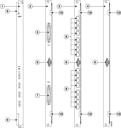
NSC front cards are available in the following configurations:
Figure 2-13 identifies the NSC front and back cards.
| 1 | NSC front card | 2 | T1E1BC-50NR back card |
| 3 | T1E1BC-RJ48 back card | 4 | T1E1BC-RED back card |
| 5 | 50-pin T1, tip and ring, transmit connector | 6 | Diagnostic port [DB9, female] |
| 7 | 50-pin T1, tip and ring, receive connector | 8 | E1 connectors, 120-ohm [RJ48] |
| 9 | Front card extractor lever | 10 | Back card extractor lever |
The NSC front card incorporates a number of status LEDs on its front panel. Figure 2-14 shows the LEDs and their labels. Table 2-5 lists the operational states associated with each LED.
| Classification/Label | Color | State | Description |
|---|---|---|---|
Card | Green | On | Illuminates steadily to indicate that the NSC is in Active mode. |
| Yellow | On | Illuminates steadily to indicate that the NSC is in Standby mode. |
| Red | On | Illuminates steadily to indicate that the NSC has failed. |
Line 1-16 | Green | On | Illuminates steadily to indicate that the DS1 interface is active and no alarms have been detected. |
| Yellow | On | Illuminates steadily to indicate that an alarm condition has been detected on the DS1 interface. |
| Red | On | Illuminates steadily to indicate that the DS1 interface is no longer handling data communication. |
| - | Off | This LED is extinguished when the DS1 interface has not been configured in the MGX 8260 database. |
|
Note Refer to the Cisco MGX 8260 Hardware Installation Guide for a comprehensive list of individual connector pinouts. |
This back card supports clock synchronization, system administration, external alarm connections and voice over IP (VoIP) call routing via Fast Ethernet ports. The SCCBC-4FE back card supports the following interface connections:
Refer to Figure 2-4, Item 2, for the locations of the connectors on this back card.
|
Note As of MGX 8260 software release 1.4, Cisco no longer supports voice over IP (VoIP) functionality for the MGX 8260. |
This back card supports clock synchronization, system administration, external alarm connections and voice over ATM (VoATM) call routing via fiber optic interfaces to multiple MGX 8850 chassis. The OC3SMIBC back card supports the following interface connections:
Refer to Figure 2-4, Item 3, for the locations of the connectors on this back card.
The T3E3DC-6DSC back card allows a DMC or BSC to make direct connections to DS3 (T1) trunks. Each trunk connection consists of separate transmit and receive SMB coaxial connectors (12 connectors per card). A serial connector (DB9) is reserved for factory diagnostics.
Refer to Figure 2-10, Item 2, for the locations of the connectors on this back card.
This back card allows NSCs to make direct connections to T1 or E1 trunks (100-ohm impedance) via shielded twisted pair (STP) copper cables to DSX patch panels or compatible termination blocks. The T1E1BC-50NR back card includes two 50-pin Champ connectors—one handles transmit pairs, the other receive pairs. It is equipped with bypass relays for automatic transfer of DS1 interfaces to a T1E1BC-RED back card. A serial connector (DB9) is reserved for factory diagnostics.
Refer to Figure 2-13, Item 2, for the locations of the connectors on this back card.
This back card allows NSCs to make direct connections to E1 trunks (120-ohm impedance) via shielded twisted pair (STP) copper cables terminated with RJ48 connectors. The T1E1BC-RJ48 back card includes 16 RJ48 connectors. It is equipped with bypass relays for automatic transfer of DS1 interfaces to a T1E1BC-RED back card. A serial connector (DB9) is reserved for factory diagnostics.
Refer to Figure 2-13, Item 3, for the locations of the connectors on this back card.
This back card enables a single NSC to function as the redundant card for other NSCs in the chassis. The T1E1BC-RED back card assumes the physical interfaces of another NSC. A serial connector (DB9) is reserved for factory diagnostics.
Refer to Figure 2-13, Item 4, for the locations of the connector on this back card.
An MGX 8260 media gateway consists of the following software components:
This subsection briefly describes these software components.
VxWorks Version 5.4 is the embedded real-time operating system (RTOS) employed by the MGX 8260 media gateway. VxWorks facilities include the following:
For additional information refer to the following documents available for download from Wind River Systems (http://www.windriver.com/products/html/vxwks54.html):
BSCs and NSCs include the software and license necessary to connect to SS7 inter-machine trunks (IMTs). An additional software license must be purchased (per BSC and NSC) to provide ISDN D channel functionality. The D channel licenses include support for non-facility associated signaling (NFAS).
The MGX 8260 includes support for an optional embedded HTML and Java device manager called WebViewer. WebViewer has an intuitive interface that facilitates managing an MGX 8260 node from a workstation via a standard Web browser. A special license must be purchased to enable this functionality. For additional information refer to the Cisco WebViewer Guide (DOC-7811012=) available from Cisco Connection On-line (CCO).
CMGM is an optional product which must be licensed per MGX 8260 node. For additional information refer to the following documents available from CCO:
![]()
![]()
![]()
![]()
![]()
![]()
![]()
![]()
Posted: Sat Sep 28 22:27:16 PDT 2002
All contents are Copyright © 1992--2002 Cisco Systems, Inc. All rights reserved.
Important Notices and Privacy Statement.