|
|

Product Numbers: CSC-3S, CSC-4S, and CSC-4T
The serial port communications interface (SCI) card provides multiple, channel-independent serial interface ports, at up to 4 megabits per second (Mbps), to the AGS+, AGS, and MGS chassis. The number of interfaces provided by the card depends on the microcode installed on the card. If the microcode version is less than 5.0, the card will provide 4 ports, each of which can operate in full-duplex (FDX) mode. If the microcode version is 5.0 or later, the card can only provide 3 ports, but each of the ports can be configured for either full- or half-duplex (HDX) operation. (HDX operation requires the Version 2 NRZI applique, which is identified by the letters "NRZI/H" on the label on the outside of the applique plate.)
The SCI card provides its serial interface ports on two 50-pin connectors. Each connector supports two synchronous serial ports. (On the three port version of the card, the second port on the second connector is disabled.) The 50-pin cable that attaches to the connector is split so that appliques of varying types can share the same cable. Figure 1 illustrates the numbering scheme for the four serial ports (labeled S0 through S3 from right to left).
| Warning Each end of the 50-pin ribbon cable is keyed for correct attachment. Reversal of the cable at either end causes permanent damage to the SCI card. |
The serial ports can be ordered with software support for low-speed (up to 64 kilobits per second [Kbps] for the three-port SCI card) or high-speed (up to 4 Mbps for the four-port SCI card only) data rates.
After installation, you can obtain information on your SCI card by using the EXEC command show controller mci. The output displays the controller type, its microcode version number, and information on the configuration of each port on the interface card.
Table 1 shows the chassis limitations of the SCI interface cards.
Table 1 Number of SCI Cards per Chassis
Note The CSC-R Token Ring interface card consumes as much power as the SCI interface card.
Therefore, if you are using both the SCI and CSC-R interfaces in any chassis, the total number of
controllers must not exceed the number indicated in
Table 2.
Table 2 Number of CSC-R Cards per Chassis
When upgrading your router from a CSC/2 processor card to a CSC/3 or CSC/4 processor card, the SCI card may require modifications for proper operation. For CSC/3 and CSC/4 compatibility, the component at location U213 should be part number 17-0675B. If you require this part, contact a service representitive for assistance.
Before installing any new cards, read this entire document for complete installation instructions and information on configuring the card for proper operation.
Before beginning any procedures, turn OFF power to the system and unplug the power cord.
Electrostatic discharge (ESD) is a discharge of stored static electricity that can damage equipment and impair electrical circuitry. It occurs when electronic components are improperly handled and can result in complete or intermittent failures.
Following are guidelines for preventing ESD damage:
For safety, periodically check the resistance value of the antistatic strap. The measurement should be between 1 and 10 mega ohms.
The sections that follow provide instructions for opening the A chassis, MGS and C chassis.
The following tools are required for accessing the chassis interior:
Access to the A chassis interior requires that you remove the front panel to access the cards or the top cover to access the rest of the chassis components. The following procedure includes instructions for both.
Before accessing the chassis interior, turn off power to the chassis and unplug the power cord because hazardous voltages may exist in or near the power supply. Use extreme caution when working near the power supply. Step 2 If the chassis is rack mounted, disconnect all external cables from the chassis rear panel. Note where these cables were connected, for reinstallation. Step 3 Remove the chassis from the rack and transfer it to a desktop or work table. Step 4 If you will need to handle any electronic components (cards, and so forth), attach appropriate ESD protection and attach the AC power cord, but to prevent a shock hazard, make certain the chassis power is OFF. Step 5 To access cards in the card cage, loosen the two thumbscrews and remove the front panel from the chassis. (See Figure 2.) If you wish to access cards in the card cage only, skip the next step. Step 6 To access other system components, locate and remove the seven No. 1 Phillips screws securing the top cover. (See Figure 2.) Set the top cover and screws aside.
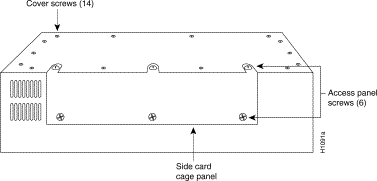
Access to the MGS chassis interior requires that you remove either the card cage access panel to access the cards or the top cover to access the rest of the chassis components. Following is the procedure for accessing the MGS chassis interior.
Step 2 If the chassis is rack mounted, disconnect all external cables from the chassis rear panel. Note where these cables were connected, for reinstallation. Step 3 Remove the chassis from the rack and transfer it to a desktop or work table. Step 4 If you need to handle any electronic components (cards, and so forth) attach appropriate ESD protection and attach the AC power cord, but to prevent a shock hazard, make certain the chassis power is OFF. Step 5 To access the cards in the card cage, locate the three flat-blade screws that secure the card cage access panel. (See Figure 3.) These screws are located on the top of the MGS chassis access panel. Step 6 Using the flat-blade screwdriver, turn each of these screws 1/4 to 1/2 turn counterclockwise until the screw pops up. Step 7 Using the No. 2 Phillips screwdriver, loosen the three screws at the bottom edge of the card cage cover. (Do not remove these screws completely.) Carefully remove the card cage cover and set it aside. Step 8 To access the other chassis components, use the No. 1 Phillips screwdriver to remove the 14 screws that secure the top cover of the chassis. (See Figure 3.) Set the top cover aside.
All SCI cards have ejectors that allow them to be easily extracted from their slots. Cards in the A-type chassis and M chassis can be accessed by removing front or side panels. Cards in the C chassis are accessed by removing the top cover.
Be sure to turn off power to the system before gaining access to and removing any cards.
To remove a card do the following:
To install the SCI card in a chassis do the following:
Step 2 Remove the card access panel (A-type and M chassis) or the top cover (C chassis) to gain access to the card cage. (See "Opening the Chassis" above.) Step 3 Select the card number by setting the appropriate dual inline package (dip) switch at location S1. (See Figure 1.) See "Card Numbering" on page 8. Step 4 Choose the appropriate clock options. These options are controlled by the jumper at locations N11 through N28. See "Mode and Clocking Options" on page 8. Step 5 Insert the SCI card in the card cage. Step 6 Attach the cables, following the cabling scheme established at the factory to ensure proper operation. Each end of the 50-pin ribbon cable is keyed for correct attachment. Reversal of the cable at either end causes permanent damage to the SCI card. The arrow on the 50-pin connector identifies pin 1.
You can also identify pin 1 and the port for each connector as follows: Lay the cable flat facing the lines down and the cable connector to the right, then pick up the connector and look at the lines on the cable. The blue line nearest you identifies pin 1 on port 0. The red line identifies pin 1 on port 1. This same scheme holds true for connections to serial ports 2 and 3. The line nearest you identifies pin 1 on port 2, and the red line identifies pin 1 on port 3.
The ends of these connectors attach to RS-232, V.35 or RS-449 appliques on the chassis rear panel. (Note that the rectangular connectors have a molded-in diamond on the connector body nearest pin-1.)
On the newer RS-232 applique, the cable between the SCI card and the applique is keyed on both ends, which means that the cable connector is installed on the serial port so the connector pins are aligned.
When making this connection with older appliques, it is important to determine the location of pin 1 for each port and match it correctly to pin 1 on the applique. If the connectors are not installed correctly, it will cause damage to the interface controller card.
Most of the internal cable connectors have built-in ejectors that snap closed automatically when the cable end is inserted. To release the cable, pull the tabs at either side of the connector away from the center of the connector.
Step 7 Power on the system for an installation check. Step 8 Check the LEDs. The SCI card contains a bank of 16 LEDs; however, only four are currently used. The LEDs listed in Figure 4 turn on when the interface acknowledges the Carrier Detect signal. See "LED Indicators" on page 10. Step 9 Replace the card access panel or the top cover.
Table 3 shows the switch (S1) settings for card numbering. The card numbers within the set of MCI and SCI cards installed in the chassis must be unique. These card numbers must also be unique among the other cards installed. Card number 0 can be used only if no ciscoBus controller card is installed; the ciscoBus controller card is card number 0 by default.
Table 3 Switch (S1) Settings for Card Numbering
01
Jumpers N22, N26, N12, and N16 control the serial ports 0 through 3 in DCE mode. In addition to changing these jumpers for DCE operation, you must configure the clock rate on each serial interface of the interface card by using the clockrate speed interface subcommand (where speed is the bit rate of the interface in bits per second [bps]). The applique must be DCE (or configured as DCE) to generate the clock signals.
Following is sample output of the clockrate speed command:
The no clockrate command removes the clock rate if data terminal equipment (DTE) mode is desired. Refer to the appropriate configuration and reference publication for more information on these commands. Following are the acceptable clockrate speed settings, appearing as they are entered with the clockrate speed command:
1200, 2400, 4800, 9600, 19200, 38400, 56000, 6400, 7200, 12500, 148000, 500000, 800000, 1000000, 1300000, 2000000, and 4000000
The fastest speeds might not work if your cable is too long. Speeds faster than 148 kbps are not recommended for RS-232 or RS-232 SDLC signaling. It is recommended that you use the RS-232 and NRZI appliques only at speeds up to 64 kbps; for speeds above 64 kbps, use RS-449, X.21, or HD V.35.
Most DTE interfaces require a Normal External Transmit Clock signal. All DCE interfaces require an Internal Transmit Clock (noninverted) signal. The clocking options are controlled by jumper areas N11 through N28.
Occasionally, delays occur between the Serial Clock Transmit External (SCTE) clock and the transmitted data that may push the data transition out to the point where using an inverted clock is appropriate (jumpers N13, N17, N23, and N27); however, an inverted clock is not recommended.
Typical delays indicate that the inverted clock may be appropriate above 1.3 megabits per
Table 4 shows the jumper settings for clock options. The last two columns of these tables (DTE and DCE) indicate the setting that should be used with either a DTE or DCE applique. Unless specifically noted, all products are shipped with the factory default setting to work with the DTE applique, which requires external clocking; the channel service unit/digital service unit (CSU/DSU) provides the clocking for the circuit. DTE operation with the NRZI applique requires a special cable (Part Number 72-0751-01, order number CAB-R232NZ=).
Table 4 Jumper Settings for Clock Options
X1
The SCI card contains a bank of 16 LEDs. (Four are currently used.) Figure 4 shows the LEDs that are used and the serial port each LED represents. At startup, all LEDs flash and then only those LEDs that indicate active interfaces will stay on. An interface is considered active if Carrier Detect (CD) is present on that serial interface and the interface is enabled. A problem is indicated if all LEDs remain on after the system boots, or if the LED of a active interface does not stay on after the system boots.
Processor Card Compatibility
Installation
Preventing Electrostatic Discharge Damage
![]()
Caution Opening the Chassis
Tools Required
Opening the A Chassis
![]()
Warning
Step 1 Turn OFF power to the chassis and unplug it from AC power.
Figure 2 Chassis Front and Top Panels
Opening the MGS
Step 1 Turn OFF power to the chassis and unplug it from AC power.
Figure 3 Screw Locations on the MGS Chassis Exterior—Side View
Removing the SCI Card
Installing the SCI Card
Step 1 Turn OFF power to the unit and unplug it.
![]()
Caution
Card Numbering
Card No.
S1-1
S1-2
S1-3
S1-4
1 Use only if no ciscoBus controller card is installed. The ciscoBus controller card is card number 0 by default.
Mode and Clocking Options
second (Mbps), depending upon the DTE clock-to-data skews and setup required, and allowing some margin for temperature, cable, and other variables. Some DCE devices will not accept SCTE, so Serial Clock Transmit (SCT) must be used. Inverting the clock may be the only way to compensate for the cable length and circuit delays in the DTE and DCE.
Jumper Pair
Signal Description
Interface
DTE
DCE
1 X = Recommended setting. x = Available but not recommended.
LED Indicators
Figure 4 LED Indicators—Partial Front-Edge View
![]()
![]()
![]()
![]()
![]()
![]()
![]()
![]()
Posted: Thu Nov 6 16:05:08 PST 2003
All contents are Copyright © 1992--2003 Cisco Systems, Inc. All rights reserved.
Important Notices and Privacy Statement.