|
|

This chapter provides the following cable assembly illustrations and pinout descriptions so you can construct your own cables.
The cables available from Cisco meet FCC RF and VDE emissions requirements. When you construct your own cables you should refer to appropriate documentation regarding interference considerations and cable length limitations.
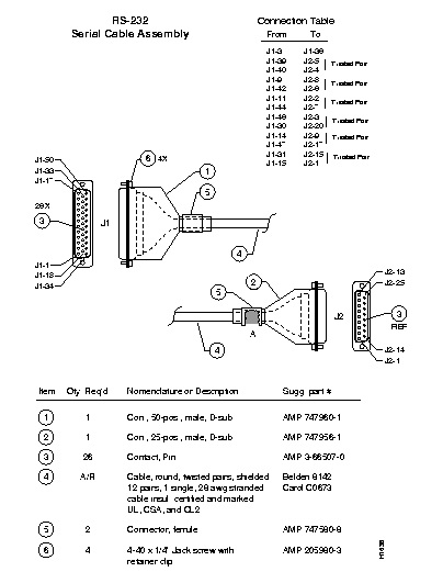
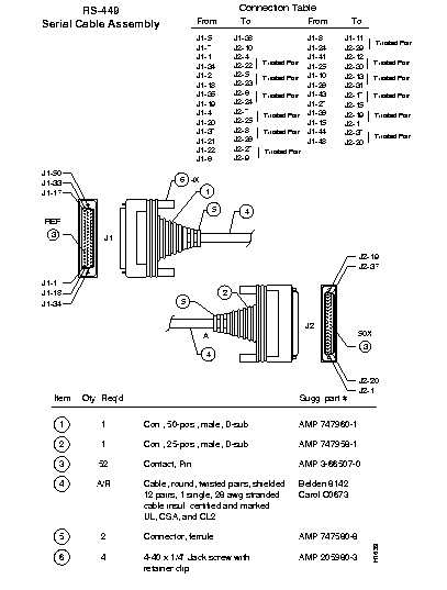
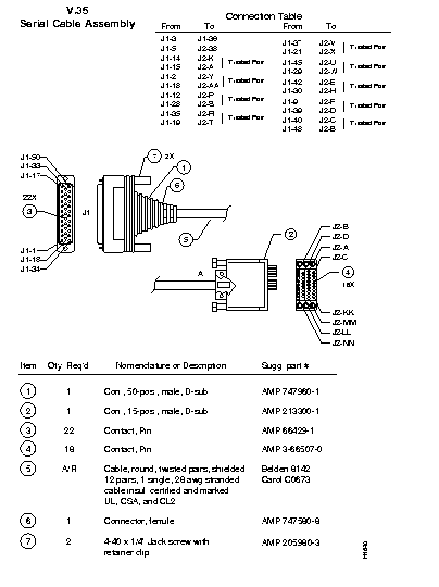
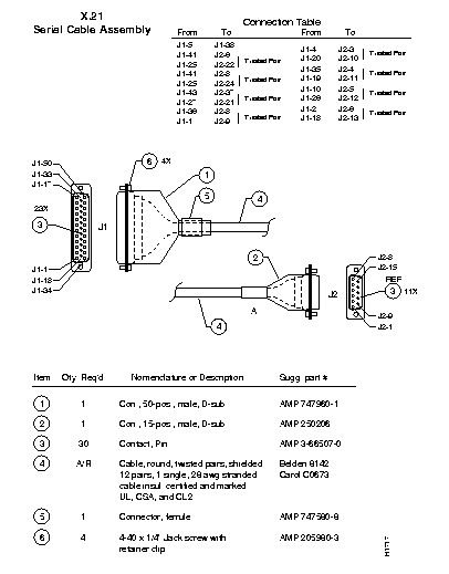
Use the following illustrations as a guide to creating your own cables. Connection tables and a list of components are provided in each of the illustrations. Suggested sources for components are also provided.
When assembling your cable, follow these steps:
Step 1: Fold back the braided shield to make electrical and mechanical connection with the metal shell on both ends. Refer to location "A" in the appropriate illustration.
Step 2: Cut unterminated wires back, insulate or ensure insulation from other conductors.
Refer to Figure 1-1 when assembling an RS-232 cable.
Refer to Figure 1-2 when assembling an RS-449 cable.
Refer to Figure 1-3 when assembling a V.35 cable.
Refer to Figure 1-4 when assembling an X.21 cable.


The following tables provide the pinouts and signal descriptions for the RS-232, RS-449, V.35, and X.21 cables.
Table 1-1 lists the RS-232 serial cable pinouts and signal descriptions.
Table 1-2 lists the RS-449 cable pinouts and signal descriptions.
Table 1-3 lists the V.35 cable pinouts and signal descriptions.
Table 1-4 lists the X.21 cable pinouts and signal descriptions.
Table 1-5 lists the Ethernet cable pinouts and signal descriptions.
| 50 Pin | 25 Pin | Signal Name | Direction |
|---|---|---|---|
| 3 | nc | Looped to pin 36 on 50-pin connector | |
| 9 | 8 | Carrier Detect | Input |
| 11 | 2 | Transmitted Data | Output |
| 14 | 9 | Loopback | Output |
| 15 | 1 | Chassis Ground | -- |
| 42 | 6 | Data Set Ready | Input |
| 30 | 20 | Data Terminal Ready | Output |
| 31 | 15 | Transmit Clock | Input |
| 36 | nc | Looped to pin 3 on 50-pin connector | |
| 39 | 5 | Clear To Send | Input |
| 40 | 4 | Requested To Send | Output |
| 44 | 7 | Signal Ground | -- |
| 46 | 3 | Received Data | Input |
| 47 | 17 | Receive Clock | Input |
| 50 Pin | 37 Pin | Signal Name | Direction |
|---|---|---|---|
| 1 | 4 | Transmitted Data + (SD A) | Output |
| 2 | 5 | Transmit Clock + (ST A) | Input |
| 4 | 7 | Request To Send + (RS A) | Output |
| 5 | nc | Looped to pin 38 on 50-pin connector | |
| 6 | 9 | Clear To Send + (CS A) | Input |
| 7 | 10 | Loopback (LL) | Output |
| 8 | 11 | Data Set Ready + (DM A) | Input |
| 10 | 13 | Carrier Detect + (RR A) | Input |
| 15 | 1 | Chassis Ground | -- |
| 18 | 23 | Transmit Clock - (ST B) | Input |
| 19 | 24 | Received Data - (RD B) | Input |
| 20 | 25 | Request To Send - (RS B) | Output |
| 21 | 26 | Receive Clock - (RT B) | Input |
| 22 | 27 | Clear To Send - (CS B) | Input |
| 24 | 29 | Data Set Ready - (DM B) | Input |
| 25 | 30 | Data Terminal Ready - (TR B) | Output |
| 27 | 35 | Transmitter Signal Element Timing - (TT B) | Output |
| 34 | 22 | Transmitted Data - (SD B) | Output |
| 35 | 6 | Received Data + (RD A) | Input |
| 36 | 19 | Signal Ground | -- |
| 37 | 8 | Receive Clock + (RD A) | Input |
| 38 | nc | Looped to pin 5 on 50-pin connector | |
| 41 | 12 | Data Terminal Ready + (TR A) | Output |
| 26 | 31 | Carrier Detect (RR B) | Input |
| 43 | 17 | Transmitter Signal Element Timing + (TT A) | Output |
| 44 | 37 | Signal Ground | -- |
| 48 | 20 | Signal Ground | -- |
| 50 Pin | 34 Pin | Signal Name | Direction |
|---|---|---|---|
| 2 | Y | Transmit Clock + | Input |
| 3 | nc | Looped to pin 36 on 50-pin connector | |
| 5 | nc | Looped to pin 38 on 50-pin connector | |
| 9 | F | Received Line Signal Detect | Input |
| 12 | P | Transmitted Data + | Output |
| 14 | K | Loopback | Output |
| 15 | A | Chassis Ground | -- |
| 18 | AA | Transmit Clock - | Input |
| 19 | T | Received Data - | Input |
| 21 | X | Receive Clock - | Input |
| 42 | E | Data Set Ready | Input |
| 28 | S | Transmitted Data - | Output |
| 29 | W | Transmitter Signal Element Timing - | Output |
| 30 | H | Data Terminal Ready | Output |
| 35 | R | Received Data + | Input |
| 36 | nc | Looped to Pin 3 on 50-pin connector | |
| 37 | V | Receive Clock + | Input |
| 38 | nc | Looped to pin 5 on 50-pin connector | |
| 39 | D | Clear To Send | Input |
| 40 | C | Request To Send | Output |
| 45 | U | Transmitter Signal Element Timing - | Output |
| 48 | B | Signal Ground | -- |
| 50 Pin | 15 Pin | Signal Name | Direction |
|---|---|---|---|
| 1 | 2 | Transmitted Data A | Output |
| 2 | 6 | Clock A | Input |
| 4 | 3 | Control A | Output |
| 5 | nc | Looped to pin 38 on 50-pin connector | |
| 6 | 5 | Indicate A | Input |
| 8 | 5 | Indicate A | Input |
| 10 | 5 | Indicate A | Input |
| 18 | 13 | Clock B | Input |
| 19 | 11 | Received Data B | Input |
| 20 | 10 | Control B | Output |
| 21 | 13 | Clock B | Input |
| 22 | 12 | Indicate B | Input |
| 24 | 12 | Indicate B | Input |
| 34 | 9 | Transmitted Data B | Output |
| 35 | 4 | Received Data A | Input |
| 36 | 8 | Signal Ground | -- |
| 37 | 6 | Clock A | Input |
| 38 | nc | Looped to pin 5 on 50-pin connector | |
| 26 | 12 | Indicate B | Input |
| Pin Number | Ethernet Circuit | Signal Name |
|---|---|---|
| 3 | DO-A | Data Out Circuit A |
| 10 | DO-B | Data Out Circuit B |
| 11 | DO-S | Data Out Circuit Shield (Jumper L24 and M24) |
| 5 | DI-A | Data In Circuit A |
| 12 | DI-B | Data In Circuit B |
| 4 | DI-S | Data In Circuit Shield (Jumper L23 and M23) |
| 7 | CO-A | Control Out Circuit A (not connected) |
| 15 | CO-B | Control Out Circuit B (not connected) |
| 8 | CO-S | Control Out Circuit Shield (not connected) |
| 2 | CI-A | Control In Circuit A |
| 9 | CI-B | Control In Circuit B |
| 1 | CI-S | Control In Circuit Shield |
| 6 | VC | Voltage Common |
| 13 | VP | Voltage Plus |
| 14 | VS | Voltage Shield (L25 and M25) |
| Shell | PG | Protective Ground |
|
|