|
|

Table Of Contents
Description of Network Clocking
Revertive and Nonrevertive Clocking
VISM/VISM-PR Card as a Clocking Source
PXM1 Card as a Clocking Source
PXM1E or PXM45 Card as Clocking Source
VISM/VISM-PR Clocking
This section explains the clocking options in the following sections:
•
Description of Network Clocking
•
•
Description of Network Clocking
Network clocking means that a clock signal is generated or derived and distributed through a node to ensure a synchronized network operation.
If a clocking problem occurs on the voice circuits, calls can be dropped. Voice quality can be diminished because of the possible echoing and "hissing" problems.
VISM/VISM-PR typically interfaces to TDM devices (for example, public or private voice switches). These voice switches usually demand a robust clocking schema in which the clock supplied to each voice switch is traceable to the clock source of every other voice switch in the network.VISM must be introduced into this kind of network in a manner which does not breakdown the clocking integrity.
Typically, a local and remote VISM/VISM-PR must be provided with clock sources which are traceable to each other and traceable to the voice switches to which they interconnect. Failure to properly set up this clocking can result in dropped calls and frequent voice quality problems.
To avoid these problems, time the entire voice network, including the VISMs and MGX switches, to a single clock source that is propagated throughout the network.
Clocking Sources
To ascertain the optimum single clock source for the network, examine the entire configuration of the MGX 8000 Series platform.
The MGX 8850 supports the following types of internal and external clock sources.
•
•
•
•
Note
Revertive and Nonrevertive Clocking
PXM1E and PXM45 support revertive or nonrevertive clocking. If your MGX switch is configured for a clock source from a BITS source or PXM line source and the source line goes into the alarm state, a revertive or nonrevertive recovery occurs.
•
•
The choice of revertive or nonrevertive clocking depends upon the processor module back card used and the clocking source specified. See Table 3-1 to ascertain if your clocking is revertive or nonrevertive in your network configuration.
To make a nonrevertive clock source usable after it has failed, you must use the cnfclksrc command on the PXM card to remove the configuration of that particular clock source, and then use the cnfclksrc command again to configure it back.
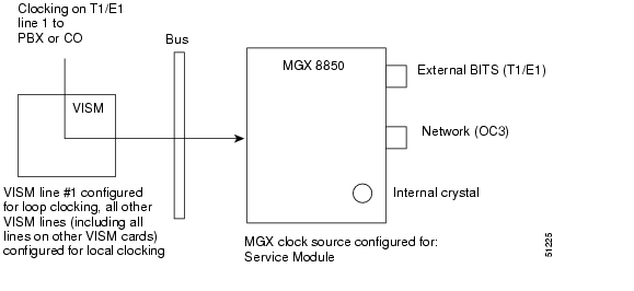
VISM/VISM-PR Card as a Clocking Source
Figure 3-1 shows the VISM card primary clocking source option, in which the clock originates at the VISM side of the VISM/PXM interface. This figure also applies to VISM-PR cards.
Figure 3-1 VISM Configured for Loop Clocking
With the VISM/VISM-PR card option, clocking originates from one of the T1 or E1 lines on one of the VISM/VISM-PR cards.
If the VISM/VISM-PR is the primary clocking source, the clocking originates on one of the VISM/VISM-PR T1 or E1 lines. The line that is providing the clock source must be configured for loop clocking. All remaining T1 or E1 lines on all of the VISM/VISM-PR cards in the shelf must be configured for local clocking.
To configure the VISM/VISM-PR card as the primary or secondary clocking source, complete the following steps:
Step 1
Step 2
Note
nodename.1.27.VISM8.a > cnfln <line_number> <line_code> <line_len> <clk_src> <line_type>
<loopback_detection> |<circuit_identifier>|
Note
Replace the cnfln arguments with the values listed in Table 3-2.
The following example shows sample syntax for adding loop clock to line 1.
nodename.1.27.VISM8.a > cnfln 1 3 9 1 3 1nodename.1.27.VISM8.a >
Note
See Chapter 10, "CLI Commands" for more information on VISM/VISM-PR commands.
Step 3
The following example shows the resulting display:
nodename.1.27.VISM8.a > dspln 1LineNum: 1LineConnectorType: RJ-48LineEnable: ModifyLineType: dsx1E1CCSLineCoding: dsx1HDB3LineLength: G.703 120 ohmLineXmtClockSource: LoopTimingLineLoopbackCommand: NoLoopLineSendCode: NoCodeLineUsedTimeslotsBitMap: 0x2LineLoopbackCodeDetection: codeDetectDisabledLineSignalingType: No SignalingLineCcsChannels: 0x0LineTrunkConditioning: disableLineBearerBusyCode: 255CircuitIdentifier:TxDigitOrder: dnisThenAniTonePlanRegion:TonePlanVersion: 0RingingTO: 180RingBackTO: 180BusyTO: 30ReorderTO: 30DialTO: 16StutterDialTO: 16OffHookAlertTO: 5RemoteRingbackMethod: proxyStep 4
Step 5
The following example shows the resulting display:
nodename.1.27.VISM8.a > dsplnsLine Conn Type Status/Coding Length XmtClock AlarmType Source---- ----- ------------ ------ -------- ------------- -------- -----27.1 RJ-48 dsx1E1CCS Mod/dsx1HDB3 G.703 120 ohm LoopTimi No27.2 RJ-48 dsx1E1CCS Mod/dsx1HDB3 G.703 120 ohm LocalTim No27.3 RJ-48 dsx1E1CCS Mod/dsx1HDB3 G.703 120 ohm LocalTim Yes27.4 RJ-48 dsx1E1CCS Mod/dsx1HDB3 G.703 120 ohm LocalTim Yes27.5 RJ-48 dsx1E1CCS Mod/dsx1HDB3 G.703 120 ohm LocalTim Yes27.6 RJ-48 dsx1E1CCS Mod/dsx1HDB3 G.703 120 ohm LocalTim Yes27.7 RJ-48 dsx1E1CCS Mod/dsx1HDB3 G.703 120 ohm LocalTim Yes27.8 RJ-48 dsx1E1CCS Mod/dsx1HDB3 G.703 120 ohm LocalTim YesLineNumOfValidEntries: 8Step 6
Step 7
nodename.1.7.PXM.a > cnfclksrc <slot.port> PReplace <slot.port> with the VISM/VISM-PR card slot number and line number of the loop clock. The P indicates that the VISM/VISM-PR card is configured as a primary clocking source.
Step 8
The following example shows the service module as the clocking source:
cvgmgx1a.1.7.PXM.a > dspclkinfo****** Clock HW registers ********SEL_T1 = t1 SEL100 = ON SEL120 = OFF SEL75 = OFFNOEXTCLK = ON NOEXTCLK2 = OFFpriMuxClockSource = SERVICE_MODULE_PRI_CLKprevPriMuxClockSource = INTERNAL_OSCprimaryInbandClockSourceLineNum = 1secMuxClockSource = INTERNAL_OSCprevSecMuxClockSource = INTERNAL_OSCsecondaryInbandClockSourceLineNumber = 1currentClockSetReq = primarycurrentClockHwStat = primaryStratumLevel = STRATUM4PreviousClockHwStat = noneextClock1Present = NoextClock2Present = NoextClkConnectorType = RJ45extClkSrcImpedance = 100 Ohmsinternal Clock Status=0, Primary Clock Status=0Secondary Clock Status=0, Last inband Clock State=0last Inband Clock state= 0, Last External Clock Present = 1Last External Clock2 Present = 1Step 9
nodename.1.7.PXM.a > cnfclksrc <slot.port> SReplace <slot.port> with the VISM/VISM-PR card slot number and line number. The S indicates that the VISM card is configured as a secondary clocking source.
Step 10
The following example shows the service module as a secondary clock source:
nodename.1.7.PXM.a > dspclkinfo****** Clock HW registers ********SEL_T1 = t1 SEL100 = ON SEL120 = OFF SEL75 = OFFNOEXTCLK = ON NOEXTCLK2 = OFFpriMuxClockSource = SERVICE_MODULE_PRI_CLKprevPriMuxClockSource = SERVICE_MODULE_PRI_CLKprimaryInbandClockSourceLineNum = 1secMuxClockSource = SERVICE_MODULE_SEC_CLKprevSecMuxClockSource = INTERNAL_OSCsecondaryInbandClockSourceLineNumber = 1currentClockSetReq = primarycurrentClockHwStat = secondaryStratumLevel = STRATUM4PreviousClockHwStat = primaryextClock1Present = NoextClock2Present = NoextClkConnectorType = RJ45extClkSrcImpedance = 100 OhmsInternal Clock Status=0, Primary Clock Status=0Secondary Clock Status=0, Last inband Clock State=0last Inband Clock state= 0, Last External Clock Present = 1Last External Clock2 Present = 1
PXM Card as Clocking Source
You can configure the PXM cards for clocking as described in the following sections:
•
•
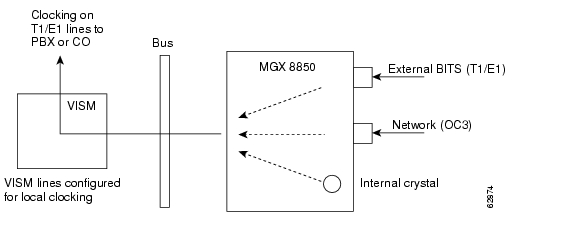
The PXM card option makes the PXM the clock source for the all cards in the chassis. The VISM/VISM-PR cards then use this clocking to provide clocking for their associated T1 or E1 lines.
PXM1 Card as a Clocking Source
Figure 3-2 shows the PXM1 card clocking source option, in which the clock originates at the PXM1 side of the VISM/PXM interface.
Figure 3-2 VISM Configured for Local Clocking
The PXM1 card option allows you to use one of the following sources:
•
•
•
To use one of the other two clocking sources, complete the following steps:
Step 1
Step 2
nodename.1.7.PXM.a > cnfclksrc <slot.port> <clktyp>Replace <slot.port> with the card slot number and line number.
Note
Replace <clktyp> with one of the following values:
•
•
•
•
Specify the cnfclksrc command argument values according to the following rules:
•
nodename.1.7.PXM.a > cnfclksrc 7.35 PType 7 for the slot number, regardless of the PXM1 card location in the chassis.
Type 35 for the port number. The BITS port is always port 35.
•
nodename.1.7.PXM.a > cnfclksrc 7.n PType 7 for the slot number, regardless of the PXM1 card location in the chassis.
Replace the n port parameter with the port number in the range 1-4.
•
•
nodename.1.7.PXM.a > cnfclksrc 7.n NType 7 for the slot number, regardless of the PXM1 card location in the chassis.
Replace n with the port number 35 or the port number, depending on which is the current source.
Type N to cancel the previous configuration and to return the clocking source to the default internal crystal.
•
nodename.1.7.PXM.a > cnfclksrc y.z PReplace the y value with the slot number of the VISM/VISM-PR card.
For VISM cards, replace z with 1 for the line argument value.
For VISM-PR cards, replace z with the line number of the clock source. Line range is 1-8.
Step 3
nodename.1.7.PXM.a > dspclkinfo****** Clock HW registers ********SEL_T1 = t1 SEL100 = ON SEL120 = OFF SEL75 = OFFNOEXTCLK = ON NOEXTCLK2 = OFFpriMuxClockSource = INTERNAL_OSCprevPriMuxClockSource = INTERNAL_OSCprimaryInbandClockSourceLineNum = 1secMuxClockSource = INTERNAL_OSCprevSecMuxClockSource = INTERNAL_OSCsecondaryInbandClockSourceLineNumber = 0currentClockSetReq = primarycurrentClockHwStat = primaryStratumLevel = STRATUM4PreviousClockHwStat = primaryextClock1Present = NoextClock2Present = NoextClkConnectorType = RJ45extClkSrcImpedance = 100 OhmsInternal Clock Status=0, Primary Clock Status=0Secondary Clock Status=0, Last inband Clock State=0last Inband Clock state= 0, Last External Clock Present = 1Last External Clock2 Present = 1Step 4
Step 5
nodename.1.27.VISM8.a > cnfln <line_number> <line_code> <line_length> <clk_src>
<line_type> <loopback_detection> |<circuit_identifier>|
Note
Replace the cnfln arguments with the values listed in Table 3-3.
The following example shows sample syntax for adding local clock to line 1.
nodename.1.27.VISM8.a > cnfln 1 3 9 2 3 1nodename.1.27.VISM8.a >Step 6
Step 7
nodename.1.27.VISM8.a > dsplnsLine Conn Type Status/Coding Length XmtClock AlarmType Source---- ----- ------------ ------ -------- ------------- -------- -----27.1 RJ-48 dsx1E1CCS Mod/dsx1HDB3 G.703 120 ohm LocalTim No27.2 RJ-48 dsx1E1CCS Mod/dsx1HDB3 G.703 120 ohm LocalTim No27.3 RJ-48 dsx1E1CCS Mod/dsx1HDB3 G.703 120 ohm LocalTim Yes27.4 RJ-48 dsx1E1CCS Mod/dsx1HDB3 G.703 120 ohm LocalTim Yes27.5 RJ-48 dsx1E1CCS Mod/dsx1HDB3 G.703 120 ohm LocalTim Yes27.6 RJ-48 dsx1E1CCS Mod/dsx1HDB3 G.703 120 ohm LocalTim Yes27.7 RJ-48 dsx1E1CCS Mod/dsx1HDB3 G.703 120 ohm LocalTim Yes27.8 RJ-48 dsx1E1CCS Mod/dsx1HDB3 G.703 120 ohm LocalTim YesLineNumOfValidEntries: 8For more information about PXM1 card clocking, refer to the Cisco MGX 8850 Edge Concentrator Installation and Configuration, Release 1.1.3 and to the Cisco MGX 8800 Series Switch Command Reference, Release 1.1.3.
PXM1E or PXM45 Card as Clocking Source
The PXM1E and PXM45 cards have two clock source configuration options:
•
•
Note
The clock source ports on the PXM-UI-S3 and PXM-UI-S3/B cards can be used to receive clock signals from either T1 or E1 lines; the card does not support both line types simultaneously. These clock ports support stratum levels 1 to 3.
Note
The following procedure describes how to configure the switch to use clock sources on the BITS ports.
Step 1
Step 2
nodename.7.PXM.a > cnfclksrc <priority> [shelf.]slot.port -bits {e1|t1} [-revertive
{enable|disable}]
Table 3-4 describes the parameters for this command.
Note
The following command example shows how to configure a primary E1 external clock source at the upper connector of the PXM1E-UI-S3. Note the command punctuation.
nodename.7.PXM.a > cnfclksrc primary 7.35 -bits e1The next example configures a primary network clock source and enables the revertive option.
nodename.7.PXM.a > cnfclksrc primary 7.36 -bits e1 -revertive enableThe last example disables the revertive function for an E1 BITS clock.
nodename.7.PXM.a > cnfclksrc primary 7.36 -bits e1 -revertive disableStep 3
nodename.8.PXM.a > dspclkparmsBITS Cable Type : Twisted PairBITS Signal Type : Data ModeThe above example shows the default BITS clock configuration parameters. The cable type can be either twisted pair or coax. The signal type can be either data mode or sync mode.
Step 4
nodename.8.PXM.a > cnfclkparms <signal type> <cable type>Replace the signal type variable with 1 to select data or with 2 to select sync. Replace the cable type variable with 1 to select twisted pair cabling or with 2 to select coaxial cabling.
Step 5
Step 6
![]()
![]()
![]()
![]()
![]()
![]()
![]()
![]()
Posted: Mon Apr 16 14:25:58 PDT 2007
All contents are Copyright © 1992--2007 Cisco Systems, Inc. All rights reserved.
Important Notices and Privacy Statement.