|
|

This appendix describes the following products that are no longer shipping as new from the factory, but are still supported in the field. These products can all be used in the chassis, but their use is either not recommended, or an improved version exists.
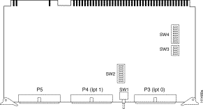
The CSC-P is a parallel printer interface card capable of controlling up to two parallel printers. The CSC-P card is obsolete, but still supported in the field. Figure F-1 shows the component-side view of the CSC-P card.

The placement of the CSC-P interface in the chassis backplane is critical for correct operation. Ensure that the CSC-ENVM card is in the top slot of the chassis and that the processor card is installed in the second slot. Install the CSC-P cards and any other bus masters (such as the CSC-R interface card) next to each other in the chassis with the CSC-P in the slot below the CSC-R (if one is installed). There must be an uninterrupted series of bus master cards in the card cage slots immediately below the processor card. Allow no gaps between these cards. Table F-1 shows the recommended card placement order for the CSC-P in the chassis backplane.
| Slot | Card |
|---|---|
| 1 | CSC-ENVM card |
| 2 | Processor card |
| 3 | Printer Card |
The CSC-P contains several switchable startup options listed in Table F-2.
| Switch | Setting | Description |
|---|---|---|
| SW1 | Center | Self-test |
| SW2 | All on | System bus address bits |
| SW3-1 | On | Select style of system bus address decoding |
| SW3-2 | - | On for unit 0, off for unit 1 |
| SW3-3 | Off | System bus address bits |
| SW3-4 | Off | System bus address bits |
| SW4-4 | On | Interrupt level of card; all other SW4 switches off |
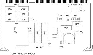
The CSC-R Token Ring interface card, shown in Figure F-2, provides interconnection to IEEE-802.5 and IBM Token Ring media. The implementation is based on the TI-TMS380 chipset and an Intel 80186 controller. The data rate for this media is a maximum of 4 megahertz (MHz) and is fully compatible with the IEEE 802.5 standard. The CSC-R card is obsolete, but still supported in the field.

The maximum number of CSC-R cards must not exceed the number indicated in Table F-3. The CSC-ENVM card in the chassis provides shared Multibus memory for the CSC-R card.
| Chassis | Max. No. of CSC-Rs |
|---|---|
| AGS+ with a CSC/3 or CSC/4 processor card | 3 |
The CSC-R card acts as a system bus master in the server. If installed, bus master cards must be an uninterrupted series of card cage slots, directly below the processor card. Install all CSC-R cards (and any other bus masters such as the CSC-P interface card) next to each other in the chassis. Allow no gaps between these cards; the EVNM card must be in the top slot in the chassis. Table F-4 shows the recommended card placement order for the CSC-R card and associated bus masters.
| Slot | Card |
|---|---|
| 1 | CSC-ENVM |
| 2 | CSC/3 or CSC/4 |
| 3 | CSC-R |
| 4 | CSC-P |
When shipped, the CSC-R card is configured as unit 0. Each CSC-R card must have a card number different from that of other CSC-R cards, but it does not have the numbering restrictions as do the CSC-R16M and CSC-MCI cards. Table F-5 shows how to change jumper area W9 to relocate the Token Ring interface to another card number.
The CSC-R card contains a number of jumpers that determine how the card operates, including two jumper blocks that set the input/output (I/O) address and the card number of this interface. Modify only these jumper blocks, where appropriate; leave all other jumper blocks at the factory-default settings.
| Card No. | A2 | A3 | A4 | A5 | A6 | A7 |
|---|---|---|---|---|---|---|
| 0 | In | In | In | Out | In | Out |
| 1 | Out | In | In | Out | In | Out |
| 2 | In | Out | In | Out | In | Out |
| 3 | Out | Out | In | Out | In | Out |
There must be a CSC-ENVM card in the system to provide shared system bus memory for the CSC-P cards, which require a minimum of 32 kilobytes. Certain combinations of CSC-R and CSC-P cards may demand more memory than the amount supplied by the CSC-ENVM card. The software automatically detects this requirement.
The V.35 DTE applique LED functions are listed in Table F-6, and the pinout is listed in Table F-7. There are no user configurable jumpers on the applique, and it can be used as DTE only at all of the data speeds supported by the MCI and SCI Multibus serial interface cards. There are no software or microcode-related limitations with this applique. The V.35 DTE applique is obsolete, but still supported in the field.
| Color | Direction DCE DTE | Mnemonic | Function |
|---|---|---|---|
| Red | --> | RxD | Receive Data |
| Red | --> | RxC | Receive Clock |
| Red | <-- | TxD | Transmit Data |
| Red | <-- | TxC | Transmit Clock |
| Red | <-- | DTR | Data Terminal Ready |
| Red | <-- | RTS | Request To Send |
| Red | --> | CTS | Clear To Send |
| Red | --> | RLSD | Receive Line Signal Detect |
| Red | <-- | LT | Local Test (software loopback) |
| Green | On if OK | +5V | +5V present |
| Green | On if OK | +12V | +12V present |
| Green | On if OK | -12V | -12V present |
| Green | On if OK | OK | Applique Test Okay |
| Pin | Direction DCE DTE | Mnemonic | Function |
|---|---|---|---|
| A | - | FG | Frame Ground |
| B | - | SG | Signal Ground |
| C | <-- | RTS | Request to Send |
| D | --> | CTS | Clear to Send |
| E | --> | DSR | Data Set Ready |
| F | --> | RLSD | Receive Line Signal Detect (Carrier Detect) |
| H | <-- | DTR | Data Terminal Ready |
| J | - | RI | Ring Indicate (not used) |
| K | <-- | LT | Local Test (Loopback) |
| R | --> | RD+ | Receive Data+ |
| T | --> | RD- | Receive Data- |
| V | --> | SCR+ | Serial Clock Receive+ |
| X | --> | SCR- | Serial Clock Receive- |
| P | <-- | SD+ | Send Data+ |
| S | <-- | SD- | Send Data- |
| U | <-- | SCTE+ | Serial Clock Transmit External+ |
| W | <-- | SCTE- | Serial Clock Transmit External- |
| Y | --> | SCT+ | Serial Clock Transmit Internal+ |
| a | --> | SCT- | Serial Clock Transmit Internal- |
|
|